Specifications
Important
Unless otherwise stated, all specifications apply after 30 minutes of instrument warm-up.
Important
An internal calibration is performed 10 minutes after powering the instrument. This internal calibration is essential to achieve the specifications of the system. Further it is required to perform the internal calibration after 7 days of instrument use. This automatic calibration is turned on by default and can be configured in the Device tab.
Important
Important changes in the specification parameters are explicitly mentioned in the revision history of this document.
General Specifications
| Parameter | min | typ | max |
|---|---|---|---|
| storage temperature | –25 °C | - | 65 °C |
| storage relative humidity (non-condensing) | - | - | 95% |
| operating temperature | 5 °C | - | 40 °C |
| operating relative humidity (non-condensing) | - | - | 90% |
| specification temperature | 18 °C | - | 28 °C |
| power consumption | - | - | 150 W |
| operating environment | IEC61010, indoor location, installation category II, pollution degree 2 | ||
| operating altitude | up to 2000 meters | ||
| power inlet fuses | 250 V, 2 A, fast acting, 5 x 20 mm | ||
| power supply AC line | 100-240 V (±10%), 50/60 Hz | ||
| dimensions with handles and feet | 45.0 x 34.5 x 10.0 cm, 17.7 x 13.6 x 3.9 inch, 19 inch rack compatible | ||
| weight | 6.4 kg | ||
| recommended calibration interval | 2 years | ||
| Parameter | min | typ | max |
|---|---|---|---|
| damage threshold Signal Input 1 and 2 | –5 V | - | +5 V |
| damage threshold Signal Output 1 and 2 | –2.5 V | - | +2.5 V |
| damage threshold Ref / Trigger 1 and 2 | –6 V | - | +6 V |
| damage threshold Trigger Out 1 and 2 | –1 V | - | +6 V |
| damage threshold Trigger In 1 and 2 | –6 V | - | +6 V |
| damage threshold Aux Output 1, 2, 3, 4 | –12 V | - | +12 V |
| damage threshold Aux In 1 and 2 | –12 V | - | +12 V |
| damage threshold DIO (digital I/O) | –1 V | - | +6 V |
| damage threshold Clk In and Clk Out | –5 V | - | +5 V |
| Parameter | Description |
|---|---|
| supported Windows operating systems | Windows 10, 11 on x86-64 |
| supported macOS operating systems | macOS 10.11+ on x86-64 and ARMv8 |
| supported Linux distributions | GNU/Linux (Ubuntu 14.04+, CentOS 7+, Debian 8+) on x86-64 and ARMv8 |
| supported processors | x86-64 (Intel, AMD), ARMv8 (e.g., Raspberry Pi 4 and newer, Apple M-series) |
| Host computer connection | Active demodulators | Maximum sample rate per demodulator | Comments |
|---|---|---|---|
| 1 GbE | 1 | 1.6 MSa/s | To achieve highest rates, it is advised to remove all other data transfer that loads the LAN/USB interface. It is recommended to check the sample loss flag (in the status tab) from time to time when using high readout rate settings. |
| 2 - 4 | 800 kSa/s | ||
| 5 - 8 | 400 kSa/s | ||
| USB 2.0 | 1 - 2 | 400 kSa/s | |
| 3 - 6 | 200 kSa/s | ||
| 7 - 8 | 100 kSa/s |
Note
The sample readout rate is the rate at which demodulated samples are transferred from the Instrument to the host computer. This rate has to be set to at least 2 times the signal bandwidth of the related demodulator in order to satisfy the Nyquist sampling theorem. As the total rate is limited by the USB/LAN interface, the maximum rate becomes smaller when the number of active demodulators is increased. This is summarized in the table above. An up-to-date and performing host computer is required to achieve these rates.
Analog Interface Specifications
| Parameter | Conditions | min | typ | max |
|---|---|---|---|---|
| connectors | - | BNC, front panel single-ended | ||
| input impedance | low value | - | 50 Ω | - |
| high value | - | 1 MΩ // 16 pF | - | |
| input frequency range | 50 Ω termination | DC | - | 600 MHz |
| input frequency range | 1 MΩ termination | DC | - | 100 MHz |
| input A/D conversion | - | 12 bit, 1.8 GSa/s | ||
| input noise amplitude | > 100 kHz, 10 mV range, 50 Ω termination | - | 4 nV/√Hz | - |
| input bias current | 50 Ω termination | - | 10 μA | - |
| 1 MΩ termination | - | - | 1 nA | |
| input full range sensitivity (10 V lock-in amplifier output) | - | 1 nV | - | 1.5 V |
| input AC ranges | - | 10 mV | - | 1.5 V |
| input range (AC + common mode) | DC coupling | –1.5 V | - | +1.5 V |
| AC coupling | –3.5 V | - | +3.5 V | |
| AC coupling cutoff frequency | 50Ω termination | - | 320 kHz | - |
| 1 MΩ termination | - | 80 Hz | - | |
| input amplitude accuracy | < 100 MHz | - | 3 % | - |
| > 100 MHz | - | 10 % | - | |
| input amplitude stability | - | - | 0.1 %/°C | - |
| input offset amplitude | with respect to range | - | - | 5% |
| input harmonic distortion (HD2/HD3) | 1 Vpp, 50 Ω termination, 10 minutes after manual input calibration < 1 MHz | - | –75 dB | - |
| < 10 MHz | - | –70 dB | - | |
| < 100 MHz | - | –60 dB | - | |
| > 100 MHz | - | –50 dB | - | |
| dynamic reserve | - | 90 dB | 100 dB | |
| Parameter | Conditions | min | typ | max |
|---|---|---|---|---|
| connectors | - | BNC, front panel single-ended | ||
| output impedance | - | - | 50 Ω | - |
| output frequency range | - | DC | - | 600 MHz |
| output rise time / fall time | 10% to 90% | - | 750 ps | - |
| output frequency resolution | - | - | 6 μHz | - |
| output phase range | - | –180 ° | - | 180 ° |
| output phase resolution | - | - | 1.0 μ° | - |
| output D/A conversion | - | 14 bit, 1.8 GSa/s | ||
| output amplitude ranges | - | ±150 mV, ±1.5 V | ||
| output DC offset range | - | ±150 mV or ±1.5 V, equal to the set output amplitude range | ||
| output power | - | - | - | 7.5 dBm |
| output amplitude accuracy | < 100 MHz | - | 2% | - |
| > 100 MHz | - | 5% | - | |
| output harmonic distortion (HD2/HD3) | 1 Vpp, 50 Ω termination, < 1 MHz | - | –70 dB | - |
| < 10 MHz | - | –70 dB | - | |
| < 100 MHz | - | –55 dB | - | |
| > 100 MHz | - | –42 dB | - | |
| output noise amplitude | > 100 kHz | - | 25 nV/√Hz | - |
| output phase noise | 10 MHz, BW = 0.67 Hz, offset 100 Hz | - | –120 dBc/Hz | - |
| 10 MHz, BW = 0.67 Hz, offset 1 kHz | - | –130 dBc/Hz | - | |
| output random jitter (RMS) | 100 MHz, 6 dBm sine | - | 4.5 ps | - |
| output offset amplitude | - | –5 mV | - | 5 mV |
| output drive current | - | - | - | 100 mA |
| Parameter | Conditions | min | typ | max |
|---|---|---|---|---|
| connectors | - | BNC, front panel bidirectional SMA, back panel input SMA, back panel output |
||
| input impedance (front and back panel) | low value | - | 50 Ω | - |
| high value | - | 1 kΩ | - | |
| input level at Ref / Trigger (front panel) and Trigger In (back panel) | low input impedance | –2.5 V | - | +2.5 V |
| high input impedance | –5 V | - | +5 V | |
| output impedance (front and back panel) | - | - | 50 Ω | - |
| output level (front and back panel) | - | - | - | 3.3 V TTL |
| input trigger hysteresis | - | - | 100 mV | - |
| internal reference mode, output of reference on UHF outputs | frequency range | 1 mHz | - | 600 MHz |
| reference orthogonality | - | 0 ° | - | |
| reference acquisition time, lock time | instantaneous | |||
| internal reference mode, output of reference on Ref / Trigger | frequency range | 1 mHz | - | 200 MHz |
| reference orthogonality | - | 0 ° | - | |
| reference acquisition time, lock time | instantaneous | |||
| external reference mode and auto reference mode, reference input at Signal Input 1 and 2 | frequency range | 10 Hz | - | 600 MHz |
| amplitude, note: for low-swing input signals the gain should be set to full-swing range to achieve best performance | 100 mV | - | - | |
| amplitude (using UHF-PID option), note: for low-swing input signals the gain should be set to full-swing range to achieve best performance | 10 mV | - | - | |
| reference acquisition time, lock time | - | - | 100 reference cycles or 1.2 ms whatever is larger | |
| external reference mode, reference input at Ref / Trigger | signal type | arbitrary, active at rising edge | ||
| frequency range | 10 Hz | - | 600 MHz | |
| amplitude | 250 mV | - | - | |
| reference acquisition time, lock time | - | - | 100 reference cycles or 1.2 ms, whatever is larger | |
Note
The UHF Instrument uses the same connectors for reference and trigger signals. This applies to input signals as well as output signals. Overall, the instrument features 2 output, 2 input, and 2 bidirectional connectors for reference and triggering purposes.
| Parameter | Details | min | typ | max |
|---|---|---|---|---|
| demodulator number | - | 8 | ||
| demodulator harmonic setting range | - | 1 | - | 1023 |
| demodulator filter time constant | - | 30 ns | - | 76 s |
| demodulator measurement bandwidth | - | 628 μHz | - | 5 MHz |
| demodulator filter slope / roll-off | - | 6, 12, 18, 24, 30, 36, 42, 48 dB/oct, consisting of up to 8 cascaded critical damping filters | ||
| demodulator output resolution | - | X, Y, R, Θ with 64-bit resolution | ||
| demodulator output sample rate (readout rate), for detailed specifications refer to Table 4 | on auxiliary outputs | - | - | 28 MSa/s |
| USB 2.0 high speed | - | - | 400 kSa/s | |
| 1GbE, 1 Gbit/s LAN | - | - | 1.6 MSa/s | |
| demodulator harmonic rejection | - | 110 dBc | - | - |
| group delay (lag time from Signal Input to Aux Output) | 30 ns time constant and 1st order filter | - | - | 3 μs |
| Parameter | Details | min | typ | max |
|---|---|---|---|---|
| auxiliary output | connectors | BNC, 4 outputs on front-panel | ||
| sampling | 28 MSa/s, 16-bit | |||
| bandwidth | - | - | 7 MHz | |
| impedance | - | 50 Ω | - | |
| amplitude | –10 V | - | 10 V | |
| resolution | 0.3 mV | - | - | |
| drive current | - | - | 100 mA | |
| auxiliary input | connectors | SMA, 2 inputs on back-panel | ||
| sampling | 400 kSa/s, 16-bit | |||
| bandwidth | - | - | 100 kHz | |
| impedance | - | 1 MΩ | - | |
| amplitude | –10 V | - | 10 V | |
| resolution | 0.3 mV | - | - | |
| Parameter | Details | min | typ | max |
|---|---|---|---|---|
| internal clock (ovenized crystal) | initial accuracy | - | ±0.5 ppm | ±1 ppm |
| long term accuracy / aging | - | - | ±0.4 ppm/year | |
| short term stability (1 s) | 0.00005 ppm | - | - | |
| short term stability (100 s) | 0.0005 ppm | - | - | |
| temperature coefficient (23° ± 5°) | - | - | ±0.03 ppm/° | |
| phase noise (at 100 Hz) | - | –130 dBc/Hz | - | |
| phase noise (at 1 kHz) | - | –140 dBc/Hz | - | |
| warm-up time | - | - | 60 s | |
| UHF-RUB Rubidium clock (option) | initial accuracy at 25° | - | - | ±0.00005 ppm |
| long term accuracy / aging | - | - a | ±5e-6 ppm/day ±0.00005 ppm/year |
|
| short term stability, AVAR (1 s) | 0.00008 ppm | - | - | |
| short term stability, AVAR (100 s) | 0.000008 ppm | - | - | |
| temperature coefficient (25° ± 25°) | - | - | ±0.00005 ppm/° | |
| phase noise (at 100 Hz) | - | - | - | |
| phase noise (at 1 kHz) | - | –140 dBc/Hz | - | |
| warm-up time | - | - | 300 s @ 25°C | |
| clock input | connector 3.+ | SMA, on back-panel | ||
| impedance | - | 50 Ω | - | |
| amplitude | 200 mV | 320 mV | 1 V | |
| frequency | 9.98 MHz | 10 MHz | 10.02 MHz | |
| clock output | connector 3.+ | SMA, on back-panel | ||
| impedance | - | 50 Ω | - | |
| amplitude, 50 Ω | 250 mV | 500 mV | 1 V | |
| frequency | - | 10 MHz | - |
Digital Interface Specifications
| Parameter | Description |
|---|---|
| host computer connection | USB 2.0 high-speed, 480 Mbit/s |
| 1GbE, LAN / Ethernet, 1 Gbit/s | |
| DIO port | 4 x 8 bit, general purpose digital input/output port, 5 V TTL specification |
| ZCtrl peripheral port | 2 connectors for ZI proprietary bus to control external peripherals |
DIO Port
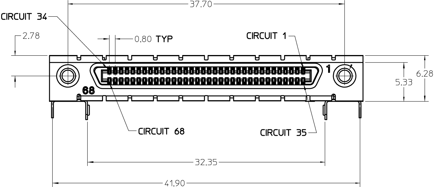
The DIO port is a VHDCI 68 pin connector as introduced by the SPI-3 document of the SCSI-3 specification. It is a female connector that requires a 32 mm wide male connector. The DIO port features 32 bits that can be configured byte-wise as inputs or outputs.
| Parameter | Details | Min | Typ | Max |
|---|---|---|---|---|
| output series termination | DO | low impedance (CMOS output) | ||
| output series termination | DOL | 33 Ω | ||
| input termination | DI, CLKI | high impedance (CMOS input) | ||
| high-level input voltage VIH | DI, CLKI | 2.0 V | - | - |
| low-level input voltage VIL | DI, CLKI | - | - | 0.8 V |
| high-level output voltage VOH | DO, at IOH < 24 mA | 4.2 V | - | - |
| high-level output voltage VOH | DOL, at IOH < 32 mA | 3.8 V | - | - |
| low-level output voltage VOL | DO, at IOL < 24 mA | - | - | 0.55 V |
| low-level output voltage VOL | DOL, at IOL < 32 mA | - | - | 0.55 V |
| high-level output current IOH (sourcing) | DO | - | - | 24 mA |
| high-level output current IOH (sourcing) | DOL | - | - | 32 mA |
| low-level output current IOL (sinking) | DO | - | - | 24 mA |
| low-level output current IOL (sinking) | DOL | - | - | 32 mA |
| Pin | Name | Description | Range specification |
|---|---|---|---|
| 68 | CLKI | clock input, used to latch signals at the digital input ports - can also be used to retrieve digital signals from the output port using an external sampling clock | 5 V CMOS/TTL |
| 67 | DOL | DIO output latch, 56.25 MHz clock signal, the digital outputs are synchronized to the falling edge of this signal | 5 V CMOS |
| 66-59 | DI[31:24] | digital input or output (set by user) | output CMOS 5 V, input is CMOS/TTL |
| 58-51 | DIO[23:16] | digital input or output (set by user) | output CMOS 5 V, input is CMOS/TTL |
| 50-43 | DIO[15:8] | digital input or output (set by user) | output CMOS 5 V, input is CMOS/TTL |
| 42-35 | DIO[7:0] | digital input or output (set by user) | output CMOS 5 V, input is CMOS/TTL |
| 34-1 | GND | digital ground | - |
The figure below shows the architecture of the DIO input/output. The DIO port features 32 bits that can be configured byte-wise as inputs or outputs by means of a drive signal. The digital output data is latched synchronously with the falling edge of the internal clock, which is running at 56.25 MHz. The internal sampling clock is available at the DOL pin of the DIO connector. Digital input data can either be sampled by the internal clock or by an external clock provided through the CLKI pin. A decimated version of the input clock is used to sample the input data. The Decimation unit counts the clocks to decimation and then latches the input data. The default decimation is 5625000, corresponding to a digital input sampling rate of 1 sample per second.

ZCtrl Peripheral Port
The ZCtrl port serves to power and communicate to external equipment, such as pre-amplifiers: the port provides a floating power supply with ±14.5 V and 100 mA per port. After Instrument power-on, the port is not active and must be switched on in order to be used. Two activation methods are supported:
- Manual switch in the user interface
- Manual switch by shorting the ZCtrl_Detect and Device_Ground - these pins should be floating against ZCtrl_GND and ZCtrl_PWR
Th ZCtrl port can be connected with an RJ45 connector, therefore non-crossed Ethernet cables can be used for convenient interfacing.
Warning
Connection to a Ethernet might damage the UHF Instrument.

| Pin | Name | Description | Range specification |
|---|---|---|---|
| 1 | ZCtrl_Power+ | power pin, for external use | 14.5 V, 100 mA |
| 2 | ZCtrl_Detect | connection detection | - |
| 3 | Device_Ground | ground of UHF Instrument, connected to earth pin | - |
| 4 | ZCtrl_Power– | power pin, for external use | –14.5 V, 100 mA |
| 5 | ZCtrl_D | proprietary function | - |
| 6 | ZCtrl_C | proprietary function | - |
| 7 | ZCtrl_GND | floating input | - |
| 8 | ZCtrl_GND | reference ground pin for ZCtrl_Power+ and ZCtrl_Power– | - |
Performance Diagrams
Many of the parameters mentioned in Analog Interface Specifications are valid without specific conditions. Other parameters instead are typical specifications, because they depend on several parameters, such as the input range setting, the input termination and/or the frequency. This section completes the previous chapters with detailed performance diagrams in order to support the validation of applications.

Input noise amplitude depends on several parameters, and in particular on the frequency and the input range setting. The input noise is lower for smaller input ranges, and it is recommended to use small ranges especially for noise measurements. Only the noise with DC input coupling is shown here as the input noise with AC coupling is the same, as long as the frequency is above the AC cutoff frequency (see Table 5).
The input noise does depend on the input impedance setting, which can be 50 Ω or 1 MΩ. The performance diagrams for 50 Ω and 1 MΩ input impedance are shown in Figure 4 and in Figure 5, respectively. For both, the corner frequency of the 1/f noise is in the range of 100 kHz. For 50 Ω input impedance, the white noise floor is around 4 nV/√Hz for the smallest input range. For 1 MΩ input impedance, the white noise floor is below 8 nV/√Hz for the smallest input range.

Figure 6 shows a typical SSB phase noise measured at the signal output. For this measurement, the UHF instrument was connected to a phase noise analyzer and the signal output amplitude was set to 1.5 V. The phase noise at 10 MHz at 10 kHz offset is around -139 dBc/Hz. The phase noise at 100 MHz at 10 kHz offset is around -118 dBc/Hz.

Clock 10 MHz
A 10 MHz clock input and output is provided for synchronization with other instruments. The figure explains the internal routing of the different clock signals. An internal clock generation unit receives a 10 MHz clock reference and generates all necessary internal sampling clocks. The clock reference either comes from the internal quartz/Rubidium oscillator or from an external clock source connected to the Clock 10 MHz In connector. The user can define if the clock is taken from the internal or external source. The Clock 10 MHz Out connector always provides the 10 MHz clock of the internal quartz/Rubidium oscillator.

Auto Calibration
The instrument requires a self calibration after a short warm-up period to ensure operation according to specifications. During this self calibration process, components of the sensitive analog front-end are calibrated to account for temperature variations and drift. The self calibration is not to be confused with the Instrument Calibration service by Zurich Instruments. The latter is performed at the manufacturer site. The self calibration lasts about one second and only applies a fine-tuning.
The first self calibration after warm-up is executed automatically. Any
further self calibration needs to be manually executed by the user. The
self calibration process can be executed by clicking the  button of the Auto Calibration section in the Device tab of the user
interface.
button of the Auto Calibration section in the Device tab of the user
interface.
The user can disable the calibration procedure completely if necessary. This can be done by changing the Enable button of the Auto Calibration in the Device tab. If this flag is disabled, no calibration is executed after warm-up time.
The default self calibration procedure can be divided into three different states, which are also indicated by the CAL flag in the footer of the user interface. The CAL flag can be either yellow, gray/off, or red.
- Yellow: The yellow CAL flag indicates that the calibration has not been executed yet. After a warm-up and temperature settling period of approximately 16 minutes, a self calibration is executed and the CAL flag turns gray. If the self calibration is disabled, the CAL flag turns red after the warm-up period to indicate that no calibration was performed.
- Gray/off: The gray CAL flag indicates that the instrument is self calibrated. The CAL flag turns red when the temperature change is larger than a given threshold or the time since the last calibration is longer than a given time interval. The values of these thresholds are indicated in the Device tab.
- Red: The red CAL flag indicates that it is recommended to perform a self calibration. The self calibration is never executed automatically in this state. The CAL flag is red, either, when the instrument experienced a temperature change larger than a given threshold, or when the time since the last calibration is longer than a given time interval. By executing a self calibration, the CAL flag will turn gray.