Specifications
Important
Unless otherwise stated, all specifications apply after 30 minutes of instrument warm-up.
Important
Important changes in the specification parameters are explicitly mentioned in the revision history of this document.
General Specifications
| Parameter | Min | Typ | Max |
|---|---|---|---|
| storage temperature | –25 °C | - | 65 °C |
| storage relative humidity (non-condensing) | - | - | 95% |
| operating temperature | 5 °C | - | 40 °C |
| operating relative humidity (non-condensing) | - | - | 90% |
| specification temperature | 18 °C | - | 28 °C |
| power consumption | - | - | 250 W |
| operating environment | IEC61010, indoor location, installation category II, pollution degree 2 | ||
| operating altitude | up to 2000 meters | ||
| power inlet fuses | 250 V, 3 A, fast acting, 5 x 20 mm | ||
| power supply AC line | 100-240 V (±10%), 50/60 Hz | ||
| dimensions including bumper | 23.2 × 10.2 × 43.0 cm, 9.2 × 4.0 ×16.9 inch, 19 inch rack compatible | ||
| weight | 4.6 kg | ||
| recommended calibration interval | 2 years | ||
| Parameter | Min | Typ | Max |
|---|---|---|---|
| damage threshold Wave Out (direct) | –1.2 V | - | +1.2 V |
| damage threshold Wave Out (amplified) | –6 V | - | +6 V |
| damage threshold Mark Out | –0.7 V | - | +4 V |
| damage threshold Trig In (1 kΩ input impedance) | –11 V | - | +11 V |
| damage threshold Trig In (50 Ω input impedance) | –6 V | - | +6 V |
| damage threshold Reference Clk In (DC) | –4 V | - | +4 V |
| damage threshold Reference Clk In (AC, with DC offset 0 V) | - | - | +13.5 dBm |
| damage threshold Reference Clk Out (DC) | –4 V | - | +4 V |
| damage threshold Sample Clk In (DC) | –4 V | - | +4 V |
| damage threshold Sample Clk In (AC, with DC offset 0 V) | - | - | +13.5 dBm |
| damage threshold Sample Clk Out (DC) | –4 V | - | +4 V |
| MDS In / Out | –0.7 V | - | +4 V |
| DIO In / Out in default configuration 3.3 V CMOS/TTL | –0.7 V | - | +4 V |
| Parameter | Description |
|---|---|
| supported Windows operating systems | Windows 10, 11 on x86-64 |
| supported macOS operating systems | macOS 10.11+ on x86-64 and ARMv8 |
| supported Linux distributions | GNU/Linux (Ubuntu 14.04+, CentOS 7+, Debian 8+) on x86-64 and ARMv8 |
| supported processors | x86-64 (Intel, AMD), ARMv8 (e.g., Raspberry Pi 4 and newer, Apple M-series) |
Analog Interface Specifications
| Parameter | Details | Min | Typ | Max |
|---|---|---|---|---|
| connectors | - | SMA, front panel single-ended | ||
| output impedance | - | - | 50 Ω | - |
| output coupling | - | DC | ||
| output modes | - | amplified, direct | ||
| output range | amplified, into 50 Ω | ±0.1 V | - | ±2.5 V |
| amplified, into 50 Ω, instruments with max. range 3 V as indicated on front panel | ±0.1 V | - | ±1.5 V | |
| direct, into 50 Ω | - | ±0.4 V | - | |
| output level accuracy | amplified, into 50 Ω | - | ±(1% of setting + 5 mVpp) | - |
| output level resolution | - | <0.1 mV | - | |
| output offset voltage | amplified, into 50 Ω (double into high impedance) | –1.25 V | - | +1.25 V |
| direct, into 50 Ω | - | 0 V | - | |
| output offset voltage accuracy | amplified, into 50 Ω (double into high impedance) | - | ±(1% of setting + 5 mV) | - |
| D/A converter vertical resolution | - | 16 bit | ||
| output phase noise | amplified, 1 Vpp, 100 MHz, offset 10 kHz | - | –135 dBc/Hz | - |
| amplified, 1 Vpp, 100 MHz, offset 1 MHz | - | –148 dBc/Hz | - | |
| direct, 0.5 Vpp, 100 MHz, offset 10 kHz | - | –135 dBc/Hz | - | |
| direct, 0.5 Vpp, 100 MHz, offset 1 MHz | - | –148 dBc/Hz | - | |
| output voltage noise density | amplified, 5 V range, > 200 kHz, into high impedance | - | 35 nV/√Hz | - |
| direct, > 200 kHz, into high impedance | - | 12 nV/√Hz | - | |
| amplified, 5 V range, 1 Hz, into high impedance | - | 4 µV/√Hz | - | |
| output RMS voltage noise | amplified, 5 V range, integrated from 100 Hz to 600 MHz, into 50 Ω | - | 320 µVrms | - |
| direct, integrated from 100 Hz to 600 MHz, into 50 Ω | - | 100 µVrms | - | |
| output spurious free dynamic range (excluding harmonics) | amplified, 1 Vpp carrier, 100 MHz, range 1 MHz to 1.2 GHz | - | 80 dBc | - |
| direct, 0.8 Vpp carrier, 100 MHz, range 1 MHz to 1.2 GHz | - | 80 dBc | - | |
| output worst harmonic component (carrier frequency <100 MHz) | amplified, 0.8 V range, 0.2 Vpp carrier | - | –65 dBc (HD2) | - |
| amplified, 0.8 V range, 0.8 Vpp carrier | - | –56 dBc (HD3) | - | |
| amplified, 1 V range, 1 Vpp carrier | - | –65 dBc (HD2) | - | |
| amplified, 2 V range, 2 Vpp carrier | - | –57 dBc (HD3) | - | |
| amplified, 3 V range, 3 Vpp carrier | - | –53 dBc (HD3) | - | |
| amplified, 4 V range, 4 Vpp carrier | - | –50 dBc (HD3) | - | |
| amplified, 5 V range, 5 Vpp carrier | - | –47 dBc (HD3) | - | |
| direct, 0.5 Vpp carrier | - | –59 dBc (HD2) | - | |
| direct, 0.8 Vpp carrier | - | –53 dBc (HD2) | - | |
| output 2nd harmonic HD2 (carrier frequency <100 MHz) | amplified, 1 V range, 1 Vpp carrier | - | –65 dBc | - |
| amplified, 5 V range, 5 Vpp carrier | - | –65 dBc | - | |
| direct, 0.8 V range, 0.5 Vpp carrier | - | –59 dBc | - | |
| output 3rd harmonic HD3 (carrier frequency <100 MHz) | amplified, 1 V range, 1 Vpp carrier | - | –65 dBc | - |
| amplified, 5 V range, 5 Vpp carrier | - | –47 dBc | - | |
| direct, 0.8 V range, 0.5 Vpp carrier | - | –73 dBc | - | |
| Parameter | Details | Min | Typ | Max |
|---|---|---|---|---|
| Wave output bandwidth (–3dB) corrected for sin(x)/x roll-off | amplified, 5.0 Vpp in 50 Ω | - | 300 MHz | - |
| direct, 0.8 Vpp 50 Ω | - | 750 MHz | - | |
| Wave output bandwidth (–3dB) corrected for sin(x)/x roll-off (instruments with max. range 3 V as indicated on front panel) | amplified, 3.0 Vpp in 50 Ω | - | 300 MHz | - |
| direct, 0.8 Vpp 50 Ω | - | 750 MHz | - | |
| D/A converter sampling rate | base sampling clock | 100 MSa/s | - | 2.4 GSa/s |
| clock rate division (powers of 2) | 20 | - | 213 | |
| internal sampling clock frequency resolution | - | - | 7 digits | - |
| Wave output rise time 20% to 80% | amplified, 0.8 V range, 0.2 V step | - | 450 ps | - |
| amplified, 5 V range, 1 V step | - | 800 ps | - | |
| amplified, 5 V range, 5 V step | - | 1100 ps | - | |
| direct, 0.8 V step | - | 300 ps | - | |
| Wave output rise time 20% to 80% (instruments with max. range 3 V as indicated on front panel) | 1 V step, amplified, 3 V range | - | 550 ps | - |
| 0.8 V step, direct | - | 300 ps | - | |
| Wave output overshoot | - | - | <1% | - |
| switchable output filter bandwidth (–3dB) | amplified output path | - | 80 MHz | - |
| trigger delay to output | from Trig input to Wave output within one channel pair (1&2, 3&4, 5&6, 7&8), using playWaveDigTrigger sequencer instruction | - | 50 ns | - |
| from any Trig input to any Wave output, using waitDigTrigger sequencer instruction | - | - | 180 ns | |
| skew between outputs | between any two Wave outputs in the same output configuration | - | 200 ps | - |
| skew adjustment range | without HDAWG-SKW option | 62 / sampling rate | ||
| with HDAWG-SKW option, sampling frequency \(\ge 666.\overline{6}\) MSa/s | 62 / sampling rate | |||
| with HDAWG-SKW option, sampling frequency \(< 666.\overline{6}\) MSa/s | 1.5 ns | |||
| skew adjustment resolution | without HDAWG-SKW option | - | 1 sample clock period | - |
| with HDAWG-SKW option | - | 10 ps | - | |
| Wave output period jitter | amplified, 150 MHz square wave | - | 3 ps RMS | - |
| - | 20 ps Pk-Pk | - | ||
| direct, 150 MHz square wave | - | 3 ps RMS | - | |
| - | 20 ps Pk-Pk | - | ||
| Parameter | Details | Min | Typ | Max |
|---|---|---|---|---|
| Waveform memory per channel | without HDAWG-ME option | - | 64 MSa | - |
| with HDAWG-ME option | - | 500 MSa | - | |
| sequence length | - | - | - | 16,384 |
| waveform granularity | - | - | 16 samples | - |
| minimum waveform length | - | - | 32 samples | - |
| waveform without markers vertical resolution | - | - | 16 bit | - |
| waveform with markers vertical resolution | - | - | 14 bit | - |
| sequencer clock frequency | - | sampling rate divided by 8 | ||
| Parameter | Details | Min | Typ | Max |
|---|---|---|---|---|
| marker outputs | - | 1 per channel, SMA output on front panel, 2 marker bits per waveform | ||
| marker output high voltage | - | - | 3.3 V | - |
| marker output low voltage | - | - | 0 V | - |
| marker output impedance | - | - | 50 Ω | - |
| marker output rise time 20% to 80% | - | - | 300 ps | - |
| marker output period jitter | square wave, 100 MHz | - | 60 ps p-p | - |
| marker output skew control range | - | –23 ns | - | +30 ns |
| marker output skew control resolution | sampling rate 2.4 GHz, depends on absolute setting | - | 10 ps | - |
| reference clock output | - | SMA on back panel | ||
| reference clock output impedance | - | 50 Ω, AC coupled | ||
| reference clock output amplitude | 100 MHz into 50 Ω | - | 2 Vpp | - |
| reference clock output frequency | internal reference mode | 100 MHz | ||
| external reference mode | 10 / 100 MHz | |||
| reference clock output jitter | derived from integrated phase noise measurement (12 kHz to 200 MHz offset frequency) | - | 260 fs RMS | - |
| sampling clock output | - | SMA on back panel | ||
| sampling clock output amplitude | 2.4 GHz into 50 Ω | - | 0.8 Vpp | - |
| 1.0 GHz into 50 Ω | - | 2 Vpp | - | |
| Parameter | Details | Min | Typ | Max |
|---|---|---|---|---|
| trigger inputs | - | 1 per channel, 1 SMA on front panel | ||
| trigger input impedance | - | 50 Ω / 1 kΩ | ||
| trigger input voltage range | 50 Ω impedance | –5 V | - | 5 V |
| 1 kΩ impedance | –10 V | - | 10 V | |
| trigger input threshold range | 50 Ω impedance | –5 V | - | 5 V |
| 1 kΩ impedance | –10 V | - | 10 V | |
| trigger input threshold resolution | - | - | < 0.4 mV | - |
| trigger input threshold hysteresis | - | - | > 60 mV | - |
| trigger input min. pulse width | - | - | 5 ns | - |
| trigger input max. operating frequency | - | - | 300 MHz | - |
| reference clock input | - | SMA on back panel | ||
| reference clock input impedance | - | 50 Ω, AC coupled | ||
| reference clock input frequency | - | 10 / 100 MHz | ||
| reference clock input amplitude | - | –4 dBm | - | +13 dBm |
| Parameter | Details | Min | Typ | Max |
|---|---|---|---|---|
| internal clock type | - | TCXO | ||
| internal clock long term accuracy / aging | - | - | - | ±0.8 ppm/year |
| internal clock short term stability (1 s) | - | - | - | 0.0001 ppm |
| internal clock initial accuracy | - | - | - | ±1 ppm |
| internal clock temperature stability | –20°C to 70°C | - | - | ±0.3 ppm |
| internal clock phase noise | offset 100 Hz | - | - | –105 dBc/Hz |
| offset 1 kHz | - | - | –125 dBc/Hz | |
Digital Interface Specifications
| Parameter | Description |
|---|---|
| host computer connection | USB 3.0 |
| 1GbE, LAN / Ethernet, 1 Gbit/s | |
| DIO port | 4 x 8 bit, general purpose digital input/output port, 3.3 V TTL specification |
| ZSync peripheral port | connector for ZI proprietary bus to communicate with PQSC or QHub |
Digital Interfaces
DIO Connector
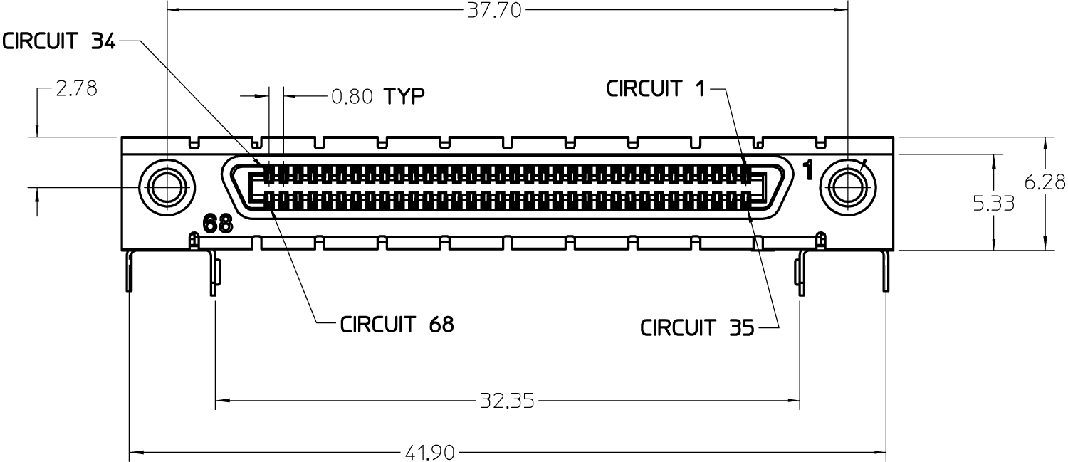
The DIO port is a VHDCI 68 pin connector as introduced by the SPI-3 document of the SCSI-3 specification. It is a female connector that requires a 32 mm wide male connector. The interface standard is switchable between LVDS (low-voltage differential signalling) and LVCMOS/LVTTL. The DIO port features 32 user-controlled bits that can all be configured byte-wise as inputs or outputs in LVCMOS/LVTTL mode, whereas in LVDS mode, half of the bits are always configured as inputs.
| Parameter | Details | Min | Typ | Max |
|---|---|---|---|---|
| supported DIO interface standards | LVCMOS/LVTTL (single-ended, 3.3 V); LVDS (differential) | |||
| output series termination | LVCMOS/LVTTL | 50 Ω (LabOne 21.02 and later) | ||
| input termination | LVCMOS/LVTTL | high impedance (logic input) | ||
| high-level input voltage VIH | LVCMOS/LVTTL | 2.0 V | - | - |
| low-level input voltage VIL | LVCMOS/LVTTL | - | - | 0.8 V |
| high-level output voltage VOH | LVCMOS/LVTTL at IOH < 12 mA | 2.6 V | - | - |
| low-level output voltage VOL | LVCMOS/LVTTL at IOL < 12 mA | - | - | 0.4 V |
| high-level output current IOH (sourcing) | LVCMOS/LVTTL | - | - | 12 mA |
| low-level output current IOL (sinking) | LVCMOS/LVTTL | - | - | 12 mA |
| input termination | LVDS | 100 Ω (differential) | ||
| input differential voltage VID | LVDS | 100 mV | - | 600 mV |
| input common-mode voltage VICM | LVDS | 0.3 V | - | 2.35 V |
| output differential voltage VOD | LVDS | 247 mV | - | 454 mV |
| output common-mode voltage VOCM | LVDS | 1.125 V | - | 1.375 V |
| Pin | Name | Description |
|---|---|---|
| 68 | CLKI | digital input |
| 67 | unused | leave unconnected |
| 66 .. 59 | DIO[31:24] | digital input or output byte (set by user) |
| 58 .. 51 | DIO[23:16] | digital input or output byte (set by user) |
| 50 .. 43 | DIO[15:8] | digital input or output byte (set by user) |
| 42 .. 35 | DIO[7:0] | digital input or output byte (set by user) |
| 34 | GND | digital ground |
| 33 | unused | leave unconnected |
| 32 .. 1 | GND | digital ground |
| Pin | Name | Description |
|---|---|---|
| 68 | CLKI+ | digital input |
| 67 | unused | leave unconnected |
| 66 .. 59 | DI+[31:24] | digital input byte |
| 58 .. 51 | DI+[23:16] | digital input byte |
| 50 .. 43 | DIO+[15:8] | digital input or output byte (set by user) |
| 42 .. 35 | DIO+[7:0] | digital input or output byte (set by user) |
| 34 | CLKI– | digital input |
| 33 | unused | leave unconnected |
| 32 .. 25 | DI–[31:24] | digital input byte |
| 24 .. 17 | DI–[23:16] | digital input byte |
| 16 .. 9 | DIO–[15:8] | digital input or output byte (set by user) |
| 8 .. 1 | DIO–[7:0] | digital input or output byte (set by user) |
DIOLink Interface
Introduction
When operating the Zurich Instruments HDAWG and UHFQA in a multi-instrument setup for quantum computing, the DIO interface can be used to communicate data within the system. There are two modes supported:
-
Operation within a Zurich Instruments Quantum Computing Control System containing a PQSC Programmable Quantum System Controller
-
Operation in a control system controlled by a third-party central controller
In the first case, the DIO interface is used to embed the UHFQA into the QCCS by a connection to a HDAWG. This case is described in the PQSC User Manual. The second mode makes use of the DIOLink interface protocol documented in the following.
The DIOLink provides a digital interface to Zurich Instruments HDAWG and UHFQA instruments. It enables the user to trigger the AWGs in the respective instruments using a digital codeword sent from a central control unit. The codeword may be used for playing back a waveform from a table with low latency, triggering a qubit measurement, etc. In case of the UHFQA instrument, the interface may also be used for communicating the results of a measurement back to the controlling unit.
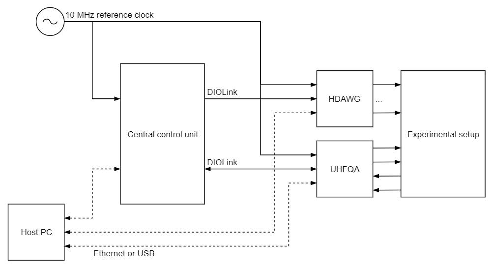
The following figure illustrates how such a measurement setup could be constructed. A host PC is responsible for controlling all the instruments in the setup. The instruments are synchronized by a shared 10 MHz reference clock. A central control unit controls the operation of the HDAWG and UHFQA instruments during experiments using the DIOLink interface. For the HDAWG, the DIOLink is unidirectional as there is rarely a need to communicate information back to the central control unit. In contrast, the DIOLink of the UHFQA is bidirectional such that measurement results can be reported back and acted upon.
For the purposes of the DIOLink, the DIO output latch (DOL) signal of the DIO connector can be ignored. The interface uses TTL signaling, which means it is sufficient to use 3.3 V for both HDAWG and UHFQA instruments in the direction from control unit to instrument. It is important to ensure that the DIOLink interface connected to a UHFQA instrument on the side of the central control unit is 5 V tolerant.
Signal Protocol
The DIOLink interface makes use of the signals shown in the following table. The signals are all transmitted from the sender to the receiver of the link. The length of the codeword varies between instruments and can at least to some extend be configured by the user.
| Name | Description |
|---|---|
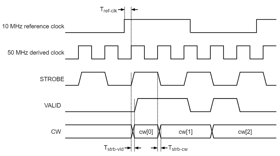
| STROBE | Toggle signal for timing alignment. The signal must toggle at a fixed rate, which defines the time grid on which codewords are transmitted. The signal is typically a 25 MHz square wave derived from the 10 MHz reference clock. |
| VALID | Codeword valid indicator. Must be asserted whenever a valid codeword is present on the DIOLink. |
| CW[N-1:0] | Codeword. The digital multi-bit codeword to be transmitted to the receiver. |
The maximum rate at which codewords can be transmitted to the instruments is 50 MHz. It is allowed to use a lower rate than 50 MHz, but the rate must always be an integer division of 50 MHz. Therefore, 25 MHz and 12.5 MHz would be supported, but 40 MHz would not. The following figure shows a timing diagram of the signaling protocol on the interface.
The timing on the interface is described in more detail in the following table.
| Name | Range | Description |
|---|---|---|
| Tref-clk | N/A | Delay from the reference clock to the clock that drives the DIOLink interface on the transmitter side. There are no specific requirements for this delay. However, it must always be the same delay every time the transmitter is activated (e.g. after powering up the instruments). |
| Tstrb-vld | ± 3.3 ns | Delay, or skew, between the STROBE and the VALID signals. |
| Tstrb-cw | ± 3.3 ns | Delay, or skew, between the STROBE and every bit of the CW signal. |
Signal Assignment HDAWG
The DIOLink signal assignment on the DIO connector to an HDAWG
instrument is freely configurable by the user. This is done using the
corresponding settings in the AWG Sequencer tab in the LabOne User
Interface. The DIO pin for the STROBE and VALID signals are selected
using Strobe Index and Valid Index settings. The codeword is specified
using the Codeword Mask and Codeword Shift settings. These two settings
allow the user to select any range up to 10 bits wide to use as an index
for playing back waveforms from a table using the playWaveDIO
sequencer instruction.
Signal Assignment UHFQA
In case of the UHFQA, the assignment of DIOLink signals to DIO pins is static and specified in the following table for those pins that communicate data from the UHFQA to the central control unit. As such, the direction is as seen from the UHFQA instrument.
| DIOLink signal | DIO pin | Direction | Description |
|---|---|---|---|
| VALID | DIO[0] | OUT | Codeword valid indicator |
| CW | DIO[10:1] | OUT | Quantized result of each of the 10 readout paths |
| reserved | DIO[13:11] | OUT | Reserved for future use |
| VALID | DIO[14] | OUT | Codeword valid indicator (same as DIO[0]) |
| STROBE | DIO[15] | OUT | Toggle signal for timing alignment, 25 MHz |
Performance Diagrams
Figure 3 shows a typical SSB phase noise measured at the signal output. For this measurement, the HDAWG was connected to a phase noise analyzer and the signal output amplitude was set to 3 V. The phase noise at 10 MHz at 1 kHz offset is around -148 dBc/Hz. The phase noise for a 100 MHz sine wave at 1 kHz offset is around -127 dBc/Hz.
