Sweeper
Note
This tutorial is applicable to all MFLI Instruments with the MF-MD Multi-demodulator option installed. The MD option is required for four-terminal measurements with simultaneous detection of voltage and current.
Goals and Requirements
This tutorial explains how to use the LabOne Sweeper to perform measurements on a MOSFET (Metal-oxide-semiconductor field-effect transistor). The goal of the tutorial is to demonstrate typical steps in the work flow of a lock-in measurement using the LabOne toolset using the MOSFET as a demonstration system. To follow this tutorial, you need a MOSFET with specifications similar to those of the IRLML2502. However, many of the working steps have a generic character and can be adopted to a multitude of transport measurement situations.
The goal of the tutorial is not to provide instructions for MOSFET characterization. This is a sophisticated measurement task and lies beyond the scope of this tutorial.
Preparation
We perform these measurement on a IRLML2502 power MOSFET manufactured by International Rectifier, but many other MOSFETs allow similar measurements with certain adjustments to the parameters. Connect the cables as shown in Figure 1. Make sure the MFLI is powered on, and then connect the MFLI through USB to your PC, or through an Ethernet cable to your local area network (LAN) where the host computer resides. After connecting to your Instrument through the web browser using its address, the LabOne graphical user interface is opened in the browser. Check the Getting Started for detailed instructions. The tutorial can be started with the default instrument configuration (e.g. after a power cycle) and the default user interface settings (i.e. as is after pressing F5 in the browser).

Tune the Gate–Source Voltage
We start by configuring the lock-in to detect the source current of the MOSFET. Open the Lock-in tab of the first demodulator. In the Reference section choose oscillator 1 and set the frequency to 1 kHz. In the Signal Input section, select Current Input 1 as the signal and set the range to 10 mA. In the Low-Pass Filter section, set the filter 3 dB bandwidth to 10 Hz.
We will operate the MOSFET with a negative drain–source offset voltage. On top of that, we apply a small alternating drain–source voltage. This is an unusual regime for the MOSFET. But it allows to operate the device in a configuration of linear response to the alternating drain–source voltage while having offset currents within the range of the MFLI Signal Input I.
In the Output Amplitudes section, set Amplitude 1 to 10 mVrms and enable the output. In the Signal Output section, set Offset to –100 mV and turn on the output. Finally, enable the data transfer of demodulator 1 in the PC Data Transfer section. The following table summarizes the settings to be made.
| Tab | Section | # | Label | Setting / Value / State |
|---|---|---|---|---|
| Lock-in | Reference | 1 | Osc | 1 |
| Lock-in | Reference | 1 | Freq | 1 kHz |
| Lock-in | Signal Input | 1 | Signal Input | Curr In 1 |
| Lock-in | Signal Input | 1 | Range | 10 mA |
| Lock-in | Low-Pass Filter | 1 | BW 3dB | 100 Hz |
| Lock-in | Output Amplitudes | 1 | Amp 1 (Vrms) | 100 mVrms |
| Lock-in | Output Amplitudes | 1 | En | On |
| Lock-in | Signal Output | 1 | Offset | –100 mV |
| Lock-in | Signal Output | 1 | On | On |
| Lock-in | PC Data Transfer | 1 | En | On |
The MOSFET gate is connected to the Auxiliary Output 1. Using the Aux tab, we can configure this output to generate a constant voltage. In the Aux Output section, set the Signal of the first Auxiliary Output to Manual. Now it is possible to output an arbitrary voltage using the Offset field. If you play around with that value while observing the MOSFET current in the Plotter or the Numeric tab, you can observe the behavior of the MOSFET as a tunable resistor. Our model is an n-channel device, therefore negative gate-source voltages lead to a suppression of the current and positive voltages of a few Volts open up the MOSFET channel. The following table summarizes the settings to be made.
Before we continue, let us shortly discuss the effect of series resistances in our measurement setup. Taking a quick glance at Figure 1 keeping in mind that Signal Input I represents a virtual ground. We would conclude that the voltage on Signal Output +V is equal to the drain–source voltage of the MOSFET, and the voltage on Auxiliary Output 1 is equal to the gate-source voltage. In reality, this is not exact, since Signal Output +V, Signal Input I, and the Auxiliary Outputs have a 50 Ω impedance connected in series internally. As soon as there is significant current flow on either of the three connectors, the actual potential at the corresponding MOSFET contact is altered. This correction is negligible for the gate contact which is essentially isolating, but it can be important for the source and drain contacts.
In the first part of the tutorial we will focus on the region with partially closed MOSFET channel. In this high-impedance configuration, we can make the assumption that currents and corrections are small. In the second part of the tutorial we will focus on the region with open MOSFET channel. In this low-impedance configuration, we instead use a four-terminal measurement to properly account for the corrections.
Sweep the Gate–Source Voltage
We will now set up a sweep of the MOSFET gate voltage. Open the Sweeper tab and in the Control sub-tab, choose Aux Out 1 Offset as Sweep Parameter. Enter Start and Stop values of 0 V and 1 V, respectively, and set Length to 100 points. Disable the Log check box so the measurement points will be linearly distributed over the interval between 0 V and 1 V.
In a Sweeper measurement, some care has to be taken in choosing a sweep speed compatible with the measurement bandwidth. If the time per point is too short, systematic errors can occur due to insufficient settling of the measurement value. You can usually let the LabOne Sweeper take care of this. Choose Application Mode in the Filter field of the Settings sub-tab. The Sweeper then chooses useful sweep parameters and adjusts the demodulator filter settings for a number of pre-defined application cases. We select the general-purpose "Parameter Sweep Averaged" case in the Application field. Please refer to Sweeper Tab for further information.
Note
It may be that the measurement bandwidth is limited by the device under test and not by the demodulator filter. The Sweeper can not account for this, as it only knows the demodulator filter bandwidth but not the properties of the device. If you’re unsure whether the sweep is too fast, check for hysteresis in the measurement by setting the Sweep Mode to Bidirectional in the Control sub-tab. If custom sweep settings appear necessary, you can access them in the Advanced Mode from the Settings sub-tab.
| Tab | Section | # | Label | Setting / Value / State |
|---|---|---|---|---|
| Sweeper | Control | Sweep Param | Aux Out 1 Offset | |
| Sweeper | Control | Start | 0 V | |
| Sweeper | Control | Stop | 1 V | |
| Sweeper | Control | Length | 100 points | |
| Sweeper | Control | Log | Off | |
| Sweeper | Settings | Filter | Application Mode | |
| Sweeper | Settings | Application | Parameter Sweep Averaged |
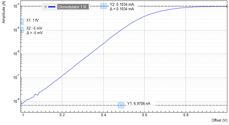
Figure 2 shows the result of the gate voltage sweep. For gate voltages below about 0.5 V, we observe an exponential suppression of the drain current. For higher voltages, the current eventually saturates at about 0.1 mA. This value is determined by the Signal Output +V amplitude of 10 mV and the cumulated 100 Ω series resistance of the MFLI input and output impedances, two times 50 Ω. Note that in this plot, the signal amplitude goes down to about 10 nA, a level of about -120 dB relative to the input range of 10 mA! This gives you an impression of the accessible dynamic range of the MFLI Instrument.
Four-Terminal Resistance Measurement
In the measurements shown so far in this tutorial, we effectively employed a two-terminal method. As long as the device under test has a large impedance, like the MOSFET with a partly closed channel, this is adequate and has the benefit of being simple. In the opposite case of small device impedance, the effect of series impedances in the cabling and Signal Outputs and Inputs, can become increasingly dominant. It is then more appropriate to employ a four-terminal method.
In our case, we may be interested in the MOSFET properties in the On state, in which its channel resistance is well below 1 Ω. In order to measure this On-resistance, we continue to measure the alternating current as we did up to now. We add a measurement of the alternating voltage drop across the MOSFET channel using the differential Signal Input of the MFLI.
We configure the second demodulator to perform this voltage measurement. Open the Lock-in tab of the second demodulator. In the Reference section, select Oscillator 1. In the Signal Input section, select Signal Input 1 and enable differential measurement by enabling the check box labeled Diff. Set the range to 1 mV and enable the data transfer of demodulator 1 in the PC Data Transfer section. The following table summarizes the settings to be made.
| Tab | Section | # | Label | Setting / Value / State |
|---|---|---|---|---|
| Lock-in | Signal Input | 2 | Sig In 1 | |
| Lock-in | Signal Input | 2 | Diff | ON |
| Lock-in | Signal Input | 2 | Range | 1 mV |
| Lock-in | Reference | 2 | Osc | 1 |
| Lock-in | PC Data Transfer | En | ON |
In order to obtain a clean four-terminal measurement, the voltages probe on the MOSFET source and drain should be as close to the device under test as possible. The best is to use point probes directly on the MOSFET contacts to eliminate the effect of soldering joint resistances.
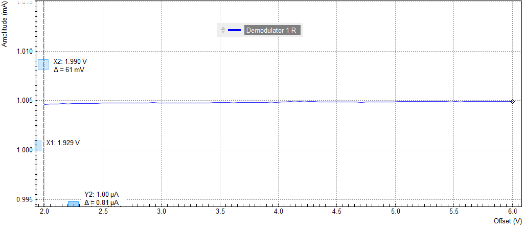
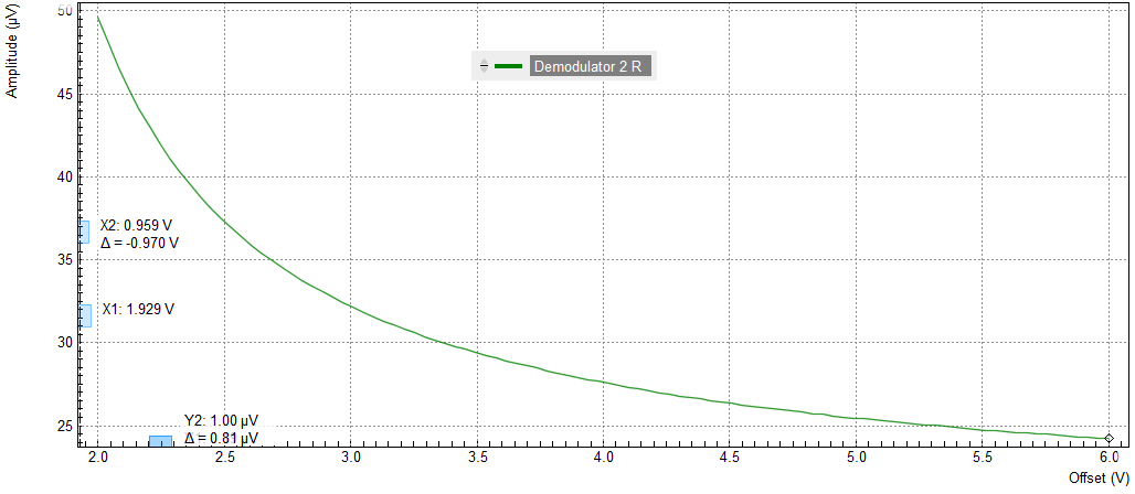
At a gate voltage (Aux Output 1) of 4 V and an excitation voltage of 100 mVrms (Signal Output 1), we can check the measurement data on the Numeric tab. We measure a source current of 1.00 mA and a source-drain voltage of 0.027 mV. This corresponds to an On-resistance of 27 mΩ in accordance with the device specifications. Figure 3 and Figure 4 show the source current and two-terminal drain–source voltage of the MOSFET over a larger gate voltage range.