Specifications
Important
Unless otherwise stated, all specifications apply after 30 minutes of instrument warm-up.
Important
An internal calibration is performed 10 minutes after powering the instrument. This internal calibration is essential to achieve the specifications of the system. Further it is required to perform the internal calibration after 7 days of instrument use. This automatic calibration is turned on by default and can be configured in the Device tab.
Important
Important changes in the specification parameters are explicitly mentioned in the revision history of this document.
General Specifications
| Parameter | min | typ | max |
|---|---|---|---|
| storage temperature | –25 °C | - | 65 °C |
| storage relative humidity (non-condensing) | - | - | 95% |
| operating temperature | 5 °C | - | 40 °C |
| operating relative humidity (non-condensing) | - | - | 90% |
| specification temperature | 18 °C | - | 28 °C |
| power consumption | - | - | 150 W |
| operating environment | IEC61010, indoor location, installation category II, pollution degree 2 | ||
| operating altitude | up to 2000 meters | ||
| power inlet fuses | 250 V, 2 A, fast acting, 5 x 20 mm | ||
| power supply AC line | 100-240 V (±10%), 50/60 Hz | ||
| dimensions with handles and feet | 45.0 x 34.5 x 10.0 cm, 17.7 x 13.6 x 3.9 inch, 19 inch rack compatible | ||
| weight | 6.4 kg | ||
| recommended calibration interval | 2 years | ||
| Parameter | min | typ | max |
|---|---|---|---|
| damage threshold Signal Input 1 and 2 | –5 V | - | +5 V |
| damage threshold Signal Output 1 and 2 | –2.5 V | - | +2.5 V |
| damage threshold Ref / Trigger 1 and 2 | –6 V | - | +6 V |
| damage threshold Trigger Out 1 and 2 | –1 V | - | +6 V |
| damage threshold Trigger In 1 and 2 | –6 V | - | +6 V |
| damage threshold Aux Output 1, 2, 3, 4 | –12 V | - | +12 V |
| damage threshold Aux In 1 and 2 | –12 V | - | +12 V |
| damage threshold DIO (digital I/O) | –1 V | - | +6 V |
| damage threshold Clk In and Clk Out | –5 V | - | +5 V |
| Parameter | Description |
|---|---|
| supported Windows operating systems | Windows 10, 11 on x86-64 |
| supported macOS operating systems | macOS 10.11+ on x86-64 and ARMv8 |
| supported Linux distributions | GNU/Linux (Ubuntu 14.04+, CentOS 7+, Debian 8+) on x86-64 and ARMv8 |
| supported processors | x86-64 (Intel, AMD), ARMv8 (e.g., Raspberry Pi 4 and newer, Apple M-series) |
Analog Interface Specifications
| Parameter | Conditions | min | typ | max |
|---|---|---|---|---|
| connectors | - | BNC, front panel single-ended | ||
| input impedance | low value | - | 50 Ω | - |
| high value | - | 1 MΩ // 16 pF | - | |
| input frequency range | 50 Ω termination | DC | - | 600 MHz |
| input frequency range | 1 MΩ termination | DC | - | 100 MHz |
| input A/D conversion | - | 12 bit, 1.8 GSa/s | ||
| input noise amplitude | > 100 kHz, 10 mV range, 50 Ω termination | - | 4 nV/√Hz | - |
| input bias current | 50 Ω termination | - | 10 μA | - |
| 1 MΩ termination | - | - | 1 nA | |
| input full range sensitivity (10 V lock-in amplifier output) | - | 1 nV | - | 1.5 V |
| input AC ranges | - | 10 mV | - | 1.5 V |
| input range (AC + common mode) | DC coupling | –1.5 V | - | +1.5 V |
| AC coupling | –3.5 V | - | +3.5 V | |
| AC coupling cutoff frequency | 50Ω termination | - | 320 kHz | - |
| 1 MΩ termination | - | 80 Hz | - | |
| input amplitude accuracy | < 100 MHz | - | 3 % | - |
| > 100 MHz | - | 10 % | - | |
| input amplitude stability | - | - | 0.1 %/°C | - |
| input offset amplitude | with respect to range | - | - | 5% |
| input harmonic distortion (HD2/HD3) | 1 Vpp, 50 Ω termination, 10 minutes after manual input calibration < 1 MHz | - | –75 dB | - |
| < 10 MHz | - | –70 dB | - | |
| < 100 MHz | - | –60 dB | - | |
| > 100 MHz | - | –50 dB | - | |
| dynamic reserve | - | 90 dB | 100 dB | |
| Parameter | Conditions | min | typ | max |
|---|---|---|---|---|
| connectors | - | BNC, front panel single-ended | ||
| output impedance | - | - | 50 Ω | - |
| output frequency range | - | DC | - | 600 MHz |
| output rise time / fall time | 10% to 90% | - | 750 ps | - |
| output frequency resolution | - | - | 6 μHz | - |
| output phase range | - | –180 ° | - | 180 ° |
| output phase resolution | - | - | 1.0 μ° | - |
| output D/A conversion | - | 14 bit, 1.8 GSa/s | ||
| output amplitude ranges | - | ±150 mV, ±1.5 V | ||
| output DC offset range | - | ±150 mV or ±1.5 V, equal to the set output amplitude range | ||
| output power | - | - | - | 7.5 dBm |
| output amplitude accuracy | < 100 MHz | - | 2% | - |
| > 100 MHz | - | 5% | - | |
| output harmonic distortion (HD2/HD3) | 1 Vpp, 50 Ω termination, < 1 MHz | - | –70 dB | - |
| < 10 MHz | - | –70 dB | - | |
| < 100 MHz | - | –55 dB | - | |
| > 100 MHz | - | –42 dB | - | |
| output noise amplitude | > 100 kHz | - | 25 nV/√Hz | - |
| output phase noise | 10 MHz, BW = 0.67 Hz, offset 100 Hz | - | –120 dBc/Hz | - |
| 10 MHz, BW = 0.67 Hz, offset 1 kHz | - | –130 dBc/Hz | - | |
| output random jitter (RMS) | 100 MHz, 6 dBm sine | - | 4.5 ps | - |
| output offset amplitude | - | –5 mV | - | 5 mV |
| output drive current | - | - | - | 100 mA |
| Parameter | Conditions | min | typ | max |
|---|---|---|---|---|
| connectors | - | BNC, front panel bidirectional SMA, back panel input SMA, back panel output |
||
| input impedance (front and back panel) | low value | - | 50 Ω | - |
| high value | - | 1 kΩ | - | |
| input level at Trigger (front panel) and Trigger In (back panel) | low input impedance | –2.5 V | - | +2.5 V |
| high input impedance | –5 V | - | +5 V | |
| output impedance (front and back panel) | - | - | 50 Ω | - |
| output level (front and back panel) | - | - | - | 3.3 V TTL |
| input trigger hysteresis | - | - | 100 mV | - |
Note
The UHF Instrument uses the same connectors for reference and trigger signals. This applies to input signals as well as output signals. Overall, the instrument features 2 output, 2 input, and 2 bidirectional connectors for reference and triggering purposes.
| Parameter | Details | min | typ | max |
|---|---|---|---|---|
| Deskew matrix | size | 2 × 2 | matrix element range | |
| –2 | - | +2 | ||
| matrix element resolution | - | - | 100e-6 | |
| sampling rate | - | 1.8 GSa/s | - | |
| Input Monitor | number of scope channels | 2 | ||
| sampling rate | - | 1.8 GSa/s | - | |
| memory | - | 2 × 4 kSa | - | |
| averages | 1 | - | 215 | |
| Integration units | number of dual-channel integrators | 10 | ||
| dual-channel integrator memory | - | 2 × 4 kSa | - | |
| sampling rate | - | 1.8 GSa/s | - | |
| trigger delay adjustment range | 0 Sa | - | 1020 Sa | |
| trigger delay resolution | - | 4 Sa | - | |
| Rotation | number of channels | 10 | ||
| data source | output of matched filters | |||
| Crosstalk Suppression matrix | size | 10 × 10 | ||
| matrix element range | –1 | - | +1 | |
| matrix element resolution | - | - | 20e-6 | |
| Signal Correlation units | number of units | 10 | ||
| data source | output of Crosstalk Suppression matrix | |||
| operation | VI,q × VI,q' for 2 outputs of Crosstalk Suppression matrix q and q' | |||
| Threshold units | number of units | 10 | ||
| data source | output of Crosstalk Suppression matrix | |||
| threshold range | –8,192 V | - | +8,192 V | |
| threshold resolution | - | - | 1e-3 V | |
| State Correlation units | number of units | 10 | ||
| data source | output of Threshold units | |||
| operation | sq × sq' for 2 outputs of Threshold units q and q' | |||
| Result Logger | number of channels | 10 | ||
| data sources | output of Rotation, Crosstalk Suppression, Signal Correlation, Threshold, State Correlation, Statistics | |||
| memory | - | 1 MSa | - | |
| averages | 1 | - | 217 | |
| Statistics units | number of units | 10 | ||
| data source | outputs of Threshold units | |||
| operations | count number of flips in bit pattern, count number of logical '1' in bit pattern, count number of state errors based on multi-qubit state map | |||
| Readout processing latency (delay between the end of a readout pulse at the Signal Inputs and the QA Result Trigger on any Trigger output) | Deskew, Rotation, and Crosstalk units bypassed | - | 140 ns | - |
| Deskew, Rotation, and Crosstalk units enabled | - | 400 ns | - | |
| Parameter | Details | min | typ | max |
|---|---|---|---|---|
| auxiliary output | connectors | BNC, 4 outputs on front-panel | ||
| sampling | 28 MSa/s, 16-bit | |||
| bandwidth | - | - | 7 MHz | |
| impedance | - | 50 Ω | - | |
| amplitude | –10 V | - | 10 V | |
| resolution | 0.3 mV | - | - | |
| drive current | - | - | 100 mA | |
| auxiliary input | connectors | SMA, 2 inputs on back-panel | ||
| sampling | 400 kSa/s, 16-bit | |||
| bandwidth | - | - | 100 kHz | |
| impedance | - | 1 MΩ | - | |
| amplitude | –10 V | - | 10 V | |
| resolution | 0.3 mV | - | - | |
| Parameter | Details | min | typ | max |
|---|---|---|---|---|
| internal clock (ovenized crystal) | initial accuracy | - | ±0.5 ppm | ±1 ppm |
| long term accuracy / aging | - | - | ±0.4 ppm/year | |
| short term stability (1 s) | 0.00005 ppm | - | - | |
| short term stability (100 s) | 0.0005 ppm | - | - | |
| temperature coefficient (23° ± 5°) | - | - | ±0.03 ppm/° | |
| phase noise (at 100 Hz) | - | –130 dBc/Hz | - | |
| phase noise (at 1 kHz) | - | –140 dBc/Hz | - | |
| warm-up time | - | - | 60 s | |
| UHF-RUB Rubidium clock (option) | initial accuracy at 25° | - | - | ±0.00005 ppm |
| long term accuracy / aging | - | - a | ±5e-6 ppm/day ±0.00005 ppm/year |
|
| short term stability, AVAR (1 s) | 0.00008 ppm | - | - | |
| short term stability, AVAR (100 s) | 0.000008 ppm | - | - | |
| temperature coefficient (25° ± 25°) | - | - | ±0.00005 ppm/° | |
| phase noise (at 100 Hz) | - | - | - | |
| phase noise (at 1 kHz) | - | –140 dBc/Hz | - | |
| warm-up time | - | - | 300 s @ 25°C | |
| clock input | connector 3.+ | SMA, on back-panel | ||
| impedance | - | 50 Ω | - | |
| amplitude | 200 mV | 320 mV | 1 V | |
| frequency | 9.98 MHz | 10 MHz | 10.02 MHz | |
| clock output | connector 3.+ | SMA, on back-panel | ||
| impedance | - | 50 Ω | - | |
| amplitude, 50 Ω | 250 mV | 500 mV | 1 V | |
| frequency | - | 10 MHz | - |
Digital Interface Specifications
| Parameter | Description |
|---|---|
| host computer connection | USB 2.0 high-speed, 480 Mbit/s |
| 1GbE, LAN / Ethernet, 1 Gbit/s | |
| DIO port | 4 x 8 bit, general purpose digital input/output port, 5 V TTL specification |
| ZCtrl peripheral port | 2 connectors for ZI proprietary bus to control external peripherals |
DIO Port
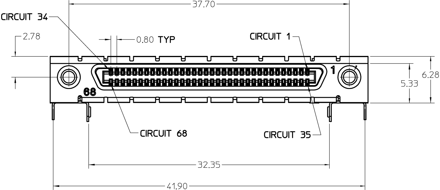
The DIO port is a VHDCI 68 pin connector as introduced by the SPI-3 document of the SCSI-3 specification. It is a female connector that requires a 32 mm wide male connector. The DIO port features 32 bits that can be configured byte-wise as inputs or outputs.
| Parameter | Details | Min | Typ | Max |
|---|---|---|---|---|
| output series termination | DO | low impedance (CMOS output) | ||
| output series termination | DOL | 33 Ω | ||
| input termination | DI, CLKI | high impedance (CMOS input) | ||
| high-level input voltage VIH | DI, CLKI | 2.0 V | - | - |
| low-level input voltage VIL | DI, CLKI | - | - | 0.8 V |
| high-level output voltage VOH | DO, at IOH < 24 mA | 4.2 V | - | - |
| high-level output voltage VOH | DOL, at IOH < 32 mA | 3.8 V | - | - |
| low-level output voltage VOL | DO, at IOL < 24 mA | - | - | 0.55 V |
| low-level output voltage VOL | DOL, at IOL < 32 mA | - | - | 0.55 V |
| high-level output current IOH (sourcing) | DO | - | - | 24 mA |
| high-level output current IOH (sourcing) | DOL | - | - | 32 mA |
| low-level output current IOL (sinking) | DO | - | - | 24 mA |
| low-level output current IOL (sinking) | DOL | - | - | 32 mA |
| Pin | Name | Description | Range specification |
|---|---|---|---|
| 68 | CLKI | clock input, used to latch signals at the digital input ports - can also be used to retrieve digital signals from the output port using an external sampling clock | 5 V CMOS/TTL |
| 67 | DOL | DIO output latch, 56.25 MHz clock signal, the digital outputs are synchronized to the falling edge of this signal | 5 V CMOS |
| 66-59 | DI[31:24] | digital input or output (set by user) | output CMOS 5 V, input is CMOS/TTL |
| 58-51 | DIO[23:16] | digital input or output (set by user) | output CMOS 5 V, input is CMOS/TTL |
| 50-43 | DIO[15:8] | digital input or output (set by user) | output CMOS 5 V, input is CMOS/TTL |
| 42-35 | DIO[7:0] | digital input or output (set by user) | output CMOS 5 V, input is CMOS/TTL |
| 34-1 | GND | digital ground | - |
The table below shows the mapping between DIO pins and input/output signals available when using the DIO connector to output qubit state measurement results. The direction is as seen from the UHFQA instrument. In order to use these signals, the Digital I/O Mode and Drive setting have to be chosen accordingly. Please refer to DIO Tab for further documentation.
| DIOLink signal | DIO pin | Direction | Description |
|---|---|---|---|
| VALID | DIO[0] | OUT | Codeword valid indicator |
| CW | DIO[10:1] | OUT | Quantized result of each of the 10 readout paths |
| reserved | DIO[13:11] | OUT | Reserved for future use |
| VALID | DIO[14] | OUT | Codeword valid indicator (same as DIO[0]) |
| STROBE | DIO[15] | OUT | Toggle signal for timing alignment, 25 MHz |
The figure below shows the architecture of the DIO input/output. The DIO port features 32 bits that can be configured byte-wise as inputs or outputs by means of a drive signal. The digital output data is latched synchronously with the falling edge of the internal clock, which is running at 56.25 MHz. The internal sampling clock is available at the DOL pin of the DIO connector. Digital input data can either be sampled by the internal clock or by an external clock provided through the CLKI pin. A decimated version of the input clock is used to sample the input data. The Decimation unit counts the clocks to decimation and then latches the input data. The default decimation is 5625000, corresponding to a digital input sampling rate of 1 sample per second.

DIOLink Interface
Introduction
When operating the Zurich Instruments HDAWG and UHFQA in a multi-instrument setup for quantum computing, the DIO interface can be used to communicate data within the system. There are two modes supported:
-
Operation within a Zurich Instruments Quantum Computing Control System containing a PQSC Programmable Quantum System Controller
-
Operation in a control system controlled by a third-party central controller
In the first case, the DIO interface is used to embed the UHFQA into the QCCS by a connection to a HDAWG. This case is described in the PQSC User Manual. The second mode makes use of the DIOLink interface protocol documented in the following.
The DIOLink provides a digital interface to Zurich Instruments HDAWG and UHFQA instruments. It enables the user to trigger the AWGs in the respective instruments using a digital codeword sent from a central control unit. The codeword may be used for playing back a waveform from a table with low latency, triggering a qubit measurement, etc. In case of the UHFQA instrument, the interface may also be used for communicating the results of a measurement back to the controlling unit.
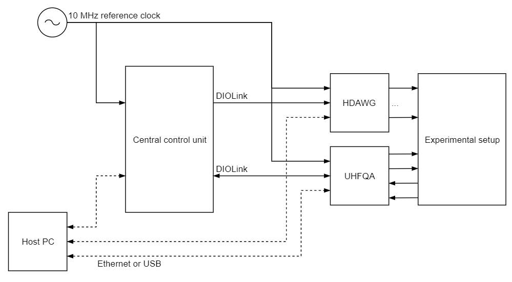
The following figure illustrates how such a measurement setup could be constructed. A host PC is responsible for controlling all the instruments in the setup. The instruments are synchronized by a shared 10 MHz reference clock. A central control unit controls the operation of the HDAWG and UHFQA instruments during experiments using the DIOLink interface. For the HDAWG, the DIOLink is unidirectional as there is rarely a need to communicate information back to the central control unit. In contrast, the DIOLink of the UHFQA is bidirectional such that measurement results can be reported back and acted upon.
For the purposes of the DIOLink, the DIO output latch (DOL) signal of the DIO connector can be ignored. The interface uses TTL signaling, which means it is sufficient to use 3.3 V for both HDAWG and UHFQA instruments in the direction from control unit to instrument. It is important to ensure that the DIOLink interface connected to a UHFQA instrument on the side of the central control unit is 5 V tolerant.
Signal Protocol
The DIOLink interface makes use of the signals shown in the following table. The signals are all transmitted from the sender to the receiver of the link. The length of the codeword varies between instruments and can at least to some extend be configured by the user.
| Name | Description |
|---|---|
| STROBE | Toggle signal for timing alignment. The signal must toggle at a fixed rate, which defines the time grid on which codewords are transmitted. The signal is typically a 25 MHz square wave derived from the 10 MHz reference clock. |
| VALID | Codeword valid indicator. Must be asserted whenever a valid codeword is present on the DIOLink. |
| CW[N-1:0] | Codeword. The digital multi-bit codeword to be transmitted to the receiver. |
The maximum rate at which codewords can be transmitted to the instruments is 50 MHz. It is allowed to use a lower rate than 50 MHz, but the rate must always be an integer division of 50 MHz. Therefore, 25 MHz and 12.5 MHz would be supported, but 40 MHz would not. The following figure shows a timing diagram of the signaling protocol on the interface.
The timing on the interface is described in more detail in the following table.
| Name | Range | Description |
|---|---|---|
| Tref-clk | N/A | Delay from the reference clock to the clock that drives the DIOLink interface on the transmitter side. There are no specific requirements for this delay. However, it must always be the same delay every time the transmitter is activated (e.g. after powering up the instruments). |
| Tstrb-vld | ± 3.3 ns | Delay, or skew, between the STROBE and the VALID signals. |
| Tstrb-cw | ± 3.3 ns | Delay, or skew, between the STROBE and every bit of the CW signal. |
Signal Assignment HDAWG
The DIOLink signal assignment on the DIO connector to an HDAWG
instrument is freely configurable by the user. This is done using the
corresponding settings in the AWG Sequencer tab in the LabOne User
Interface. The DIO pin for the STROBE and VALID signals are selected
using Strobe Index and Valid Index settings. The codeword is specified
using the Codeword Mask and Codeword Shift settings. These two settings
allow the user to select any range up to 10 bits wide to use as an index
for playing back waveforms from a table using the playWaveDIO
sequencer instruction.
Signal Assignment UHFQA
In case of the UHFQA, the assignment of DIOLink signals to DIO pins is static and specified in the following table for those pins that communicate data from the UHFQA to the central control unit. As such, the direction is as seen from the UHFQA instrument.
| DIOLink signal | DIO pin | Direction | Description |
|---|---|---|---|
| VALID | DIO[0] | OUT | Codeword valid indicator |
| CW | DIO[10:1] | OUT | Quantized result of each of the 10 readout paths |
| reserved | DIO[13:11] | OUT | Reserved for future use |
| VALID | DIO[14] | OUT | Codeword valid indicator (same as DIO[0]) |
| STROBE | DIO[15] | OUT | Toggle signal for timing alignment, 25 MHz |
ZCtrl Peripheral Port
The ZCtrl port serves to power and communicate to external equipment, such as pre-amplifiers: the port provides a floating power supply with ±14.5 V and 100 mA per port. After Instrument power-on, the port is not active and must be switched on in order to be used. Two activation methods are supported:
- Manual switch in the user interface
- Manual switch by shorting the ZCtrl_Detect and Device_Ground - these pins should be floating against ZCtrl_GND and ZCtrl_PWR
Th ZCtrl port can be connected with an RJ45 connector, therefore non-crossed Ethernet cables can be used for convenient interfacing.
Warning
Connection to a Ethernet might damage the UHF Instrument.

| Pin | Name | Description | Range specification |
|---|---|---|---|
| 1 | ZCtrl_Power+ | power pin, for external use | 14.5 V, 100 mA |
| 2 | ZCtrl_Detect | connection detection | - |
| 3 | Device_Ground | ground of UHF Instrument, connected to earth pin | - |
| 4 | ZCtrl_Power– | power pin, for external use | –14.5 V, 100 mA |
| 5 | ZCtrl_D | proprietary function | - |
| 6 | ZCtrl_C | proprietary function | - |
| 7 | ZCtrl_GND | floating input | - |
| 8 | ZCtrl_GND | reference ground pin for ZCtrl_Power+ and ZCtrl_Power– | - |
Performance Diagrams
Many of the parameters mentioned in Analog Interface Specifications are valid without specific conditions. Other parameters instead are typical specifications, because they depend on several parameters, such as the input range setting, the input termination and/or the frequency. This section completes the previous chapters with detailed performance diagrams in order to support the validation of applications.

Input noise amplitude depends on several parameters, and in particular on the frequency and the input range setting. The input noise is lower for smaller input ranges, and it is recommended to use small ranges especially for noise measurements. Only the noise with DC input coupling is shown here as the input noise with AC coupling is the same, as long as the frequency is above the AC cutoff frequency (see Table 4).
The input noise does depend on the input impedance setting, which can be 50 Ω or 1 MΩ. The performance diagrams for 50 Ω and 1 MΩ input impedance are shown in Figure 5 and in Figure 6, respectively. For both, the corner frequency of the 1/f noise is in the range of 100 kHz. For 50 Ω input impedance, the white noise floor is around 4 nV/√Hz for the smallest input range. For 1 MΩ input impedance, the white noise floor is below 8 nV/√Hz for the smallest input range.

Figure 7 shows a typical SSB phase noise measured at the signal output. For this measurement, the UHF instrument was connected to a phase noise analyzer and the signal output amplitude was set to 1.5 V. The phase noise at 10 MHz at 10 kHz offset is around -139 dBc/Hz. The phase noise at 100 MHz at 10 kHz offset is around -118 dBc/Hz.

Clock 10 MHz
A 10 MHz clock input and output is provided for synchronization with other instruments. The figure explains the internal routing of the different clock signals. An internal clock generation unit receives a 10 MHz clock reference and generates all necessary internal sampling clocks. The clock reference either comes from the internal quartz/Rubidium oscillator or from an external clock source connected to the Clock 10 MHz In connector. The user can define if the clock is taken from the internal or external source. The Clock 10 MHz Out connector always provides the 10 MHz clock of the internal quartz/Rubidium oscillator.

Device Self Calibration Procedure
The instrument requires a self calibration after a short warm-up period to ensure operation according to specifications. During this self calibration process, components of the sensitive analog front-end are calibrated to account for temperature variations and drift. The self calibration is not to be confused with the Instrument Calibration service by Zurich Instruments. The latter is performed at the manufacturer site. The self calibration lasts about one second and only applies a fine-tuning.
The first self calibration after warm-up is executed automatically. Any
further self calibration needs to be manually executed by the user. The
self calibration process can be executed by clicking the  button of the Auto Calibration section in the Device tab of the user
interface.
button of the Auto Calibration section in the Device tab of the user
interface.
The user can disable the calibration procedure completely if necessary. This can be done by changing the Enable button of the Auto Calibration in the Device tab. If this flag is disabled, no calibration is executed after warm-up time.
The default self calibration procedure can be divided into three different states, which are also indicated by the CAL flag in the footer of the user interface. The CAL flag can be either yellow, gray/off, or red.
- Yellow: The yellow CAL flag indicates that the calibration has not been executed yet. After a warm-up and temperature settling period of approximately 16 minutes, a self calibration is executed and the CAL flag turns gray. If the self calibration is disabled, the CAL flag turns red after the warm-up period to indicate that no calibration was performed.
- Gray/off: The gray CAL flag indicates that the instrument is self calibrated. The CAL flag turns red when the temperature change is larger than a given threshold or the time since the last calibration is longer than a given time interval. The values of these thresholds are indicated in the Device tab.
- Red: The red CAL flag indicates that it is recommended to perform a self calibration. The self calibration is never executed automatically in this state. The CAL flag is red, either, when the instrument experienced a temperature change larger than a given threshold, or when the time since the last calibration is longer than a given time interval. By executing a self calibration, the CAL flag will turn gray.