Signal Processing Basics
This chapter provides background knowledge about impedance measurements with a focus on the methods used by Zurich Instruments impedance analyzers. The first section explains the basic concepts behind impedance and quickly turns to the practical discussion of compensation. The remaining sections discuss subjects related to the digital lock-in technology used by the MFIA Instrument. This part of the document is of interest to users that wish to better understand signal demodulation and filtering in order to optimize their measurements for noise suppression or speed. In particular, the sinc filtering technique for low-frequency measurements is explained.
Impedance and its Measurement
Introduction
The impedance determines the electrical current flowing through a component when a voltage is applied. In general the current can be alternating at a frequency f=ω/2π and is characterized by an amplitude and a phase, and so is the voltage. The current I and voltage V can be conveniently described using complex notation, and the impedance is defined as the complex ratio Z=Z(ω)=V/I.
A measurement of a component’s impedance requires simultaneous phase-sensitive measurement of the current and voltage at the component, usually called the device under test (DUT). Zurich Instruments products employ one of two basic measurement circuits for this task: a two-terminal setup advantageous for high impedances, and a four-terminal circuit which is suitable for most situations and advantageous for low impedances. Figure 1 shows the four-terminal circuit: a drive voltage is applied to one side of the DUT. On the other side, the DUT is shorted to ground passing through a current meter. Two additional leads are connected to either side of the DUT for measuring the voltage drop across. All the current flows through the LCUR and HCUR connectors, whereas LPOT and HPOT are current-free and serve as non-invasive probes for the electrical potential. The four-terminal setup is advantageous for measuring small impedances, since it is insensitive to the effect of series impedances in the cables, connectors, soldering points, etc.

Figure 2 shows the two-terminal circuit: it is identical to the four-terminal circuit except that the voltage measurement terminals are missing. The impedance is calculated as the drive voltage divided by the measured current. This assumes that the voltage at the DUT is equal to the drive voltage, which is the case for high-impedance DUTs. The two-terminal method is advantageous in these cases because it eliminates unnecessary stray capacitances and leakage currents parallel to the DUT.

The phase sensitivity of the current and voltage measurements in Zurich Instruments impedance analyzers is accomplished by using lock-in detection. This method offers superior noise performance, large dynamic range, and high precision in phase measurements. It is explained in more detail in Principles of Lock-in Detection.
The real and imaginary parts of the impedance Z are called resistance R and reactance X, so we have Z=R+jX. Sometimes it’s more natural to express things in terms of the reciprocal of the impedance, the admittance Y=I/V=1/Z. Its real and imaginary parts are called conductance G and susceptance B, so we have Y=G+jB.
Note
In the context of lock-in amplifier measurements, it’s common to use the symbols for euclidean or polar coordinates to specify a measured quantity. For instance, a voltage V would be denoted as V=R·exp(jθ), or as V=X+jY. With Zurich Instruments impedance analyzers, V and I can be displayed directly in these terms. Consider these conventions to avoid confusion with resistance, reactance, and admittance which are denoted with the same symbols.
Ideal, Real, Measured Values
When talking about impedance, one often has in mind the cases of a resistance R, inductance L, capacitance C. The corresponding impedances are R, jωL, 1/(jωC). Components typically have nominal or ideal impedance values of a pure R, L, or C. But the impedance of any real-world component will show deviations from its ideal value. Mostly these deviations can be explained by so-called spurious impedance components. For instance, the impedance of a large resistor has a contribution due to the stray capacitance between its leads, and the contribution will be the more important the higher is the frequency. This stray capacitance lies parallel to the resistance, in this configuration it’s common to name the capacitance Cp and the resistance Rp. Recalling the law for parallel combination of impedances Ztot=1/(1/Zp1+1/Zp2), the real impedance of the resistor will be close to Zreal=1/(1/Rp+jωCp). The real impedance is furthermore not identical to the measured impedance Zmeas. The latter is what an impedance analyzer delivers, and the better the accuracy of the impedance analyzer, the closer are Zmeas and Zreal.
Circuit representations such as the parallel Cp || Rp play an important role in practical impedance measurements. Knowing the impedance Zmeas of a DUT a priori does not tell us much about the internal structure of the DUT. In order to get a deeper insight, we have to propose a realistic representation for the equivalent circuit of the DUT. Based on that, Zmeas can be split into its resistive and reactive parts, and the values of the principle and spurious component can be calculated. The main models are: - Cp || Rp (examples: large resistor with stray capacitor, capacitor with leakage current) - Cs + Rs (example: large capacitor with resistive leads) - Ls + Rs (examples: small resistor with lead inductance, inductor with wire resistance) - Lp || Rp (example: inductor with core loss)
Other, equivalent terminologies involve the dimensionless dissipation factor (loss tangent) D or the quality factor Q=1/D. A parallel combination of reactive components (such as Cp || Lp) can not be split up in an impedance measurement at a single frequency. This is why such combinations don’t appear in the list of basic circuit representations. Frequency dependence measurements allow for a detailed analysis of such circuits and other, more complex ones. Extracting the circuit type and parameters is possible by carrying out a model parameter fit of the data using specialized software such as ZView.
Test Fixtures and Compensation
When an impedance analyzer is shipped it contains an internal calibration that ensures accurate measurements at the plane of the output and input connectors. But measurements are always carried out with some sort of test fixture or cable linking the connectors to the DUT. A test fixture has its own impedance and therefore would normally distort or even invalidate the measurement of the DUT impedance. If the test fixture’s electrical characteristics are known, its spurious effect can however be calculated and largely eliminated from the measurement data. This process is called compensation. The basis for a compensation is a characterization of the test fixture through a series of standard measurements.
One generic model for a test fixture is the L/R/C/G circuit shown in Figure 3. It is a good approximation to many compact test fixtures, and it helps in getting an intuitive understanding of the properties of a test fixture and the purpose of the compensation measurement. It contains terms due to the inductance and resistance of the leads, and terms due to the stray capacitance and leakage current between the two sides of the DUT.

The compensation measurements usually consist of one or several of the following steps: - An "open" (O) step, which is a measurement of a device with infinite impedance – an open circuit - A "short" (S) step, which is a measurement of a device with zero impedance – a short circuit - A "load" (L) step, which is a measurement of a device with known impedance ideally in the desired measurement range
The "open" compensation step yields Copen and Gopen. The "short" step yields the values of Lshort and Rshort. The "load" step is required to compensate for effects that go beyond the L/R/C/G circuit. Among these effects are cable delays, or inductive cross-talk due to the mutual inductance M between the current leads (HCUR, LCUR) and the voltage (HPOT, LPOT) leads.
Optimizing the Setup
Having in mind the equivalent L/R/C/G circuit, the user setup should be optimized or chosen in view of what impedance and frequency is used. User setup here means any custom-built or commercial test fixture, or any custom-built device carrier that is plugged into the test fixture delivered with the instrument. In the regime of small impedances |ZDUT|, the series Lshort and Rshort and the mutual inductance M are most relevant. This regime applies to small resistors, capacitors at high frequencies, and inductors at low frequencies. In the regime of large impedances |ZDUT|, the parallel Copen and Gopen are most relevant. This regime applies to large resistors, capacitors at low frequencies, and inductors at high frequencies. The cable delay is always relevant when measuring at high frequencies, no matter what is the impedance. - Minimize Copen by electrostatic guarding: enclose the conductors as much as possible by grounded electrostatic guards. The corresponding "guard" connection pins are marked with a ground symbol on the MFITF test fixture. Coaxial cables provide good electrostatic guarding. For measurements of very large impedances, consider placing a guarding plate perpendicular to the axis of the DUT. - Minimize the effect of Rshort: use 4-terminal connections where the current leads (HCUR, LCUR) and the voltage leads (HPOT, LPOT) join only as close to the DUT as possible, ideally after the last soldering point. Avoid using very narrow PCB strips for current leads. - Minimize Lshort and M by magnetic guarding: allow for inductive currents to flow parallel to the current leads on the full length of the current path. Ensure a continuous guard connection along the path.
Which Compensation Method?
There are a number of different compensation methods in use, such as short-open-load (SOL), short-open (SO), or load-load-load (LLL). Independent of the combination used, some specific conditions and requirements apply to the S, O, and L steps. These are summarized in the following table.
Compensation steps:
S ("short")
- Requires "short" impedance much smaller than the DUT impedance
- sensitive to noise (small measured voltages)
O ("open")
- Requires "open" impedance much larger than the DUT impedance
- sensitive to noise (small measured currents)
- position of the electrodes identical to position with DUT
L ("load")
- "load" impedance of similar magnitude as DUT impedance recommended
- robust against noise
- accurate and stable "load" impedance required: capacitor or resistor, no inductor
The MFIA supports SOL, SO, LLL, OL, SL, L, compensation ('O' can be found in the Advanced tab). Which procedure is best suited depends first of all on the desired impedance measurement range – e.g. when aiming at measuring small impedances, a method involving a short (S) step is recommended. In contrast, an open (O) step is often not necessary. Second, it depends on the time the user is willing to spend in order to improve measurement accuracy, as every step requires a manual change of the test impedance. And third, it depends on the availability and accuracy of the test impedances, as a user compensation can only be as accurate as the available short, open, or load test impedances.
| Compensation method | Properties and use cases |
|---|---|
| SO | The short-open compensation corrects for inductive and capacitive parasitics of the user setup. This compensation method is in place if no accurate load is available, but its accuracy is limited by the fact that gain errors and cable delays can’t be compensated. |
| SL | The short-load method is a modification of the short-open method for low impedances. Gain errors and cable delays can’t be compensated. |
| OL | The open-load method is a modification of the short-open method for high impedances. Gain errors and cable delays can’t be compensated. |
| SOL | The short-open-load compensation provides very good accuracy and is recommended if an accurate load device is available. It is required if gain errors or delays need to be compensated. Non-unity gain is typically caused by cable attenuation, amplification, or attenuation by additional circuits. |
| LLL | The load-load-load method ensures the best possible accuracy in the impedance range covered by the three loads. Similarly to SOL, it allows for gain and delay compensation. It can improve on the results of the SOL method but depends on the availability of accurate load devices. |
| L | A simple compensation method offering accuracy only close to the load impedance. |
Principles of Lock-in Detection
Lock-in demodulation is a technique to measure the amplitude \(A_s\) and the phase \(\theta\) of a periodic signal with the frequency \(\omega_s = 2\pi f_s\) by comparing the signal to a reference signal. This technique is also called phase-sensitive detection. By averaging over time the signal-to-noise ratio (SNR) of a signal can be increased by orders of magnitude, allowing very small signals to be detected with a high accuracy making the lock-in amplifier a tool often used for signal recovery. For both signal recovery and phase-sensitive detection, the signal of interest is isolated with narrow band-pass filtering therefore reducing the impact of noise in the measured signal.
Figure 4 shows a basic measurement setup: a reference \(V_r\) signal is fed to the device under test. This reference signal is modified by the generally non-linear device with attenuation, amplification, phase shifting, and distortion, resulting in a signal \(V_s = A_s cos(\omega_s t + \theta_s)\) plus harmonic components.

For practical reasons, most lock-in amplifiers implement the band-pass filter with a mixer and a low-pass filter (depicted in Figure 5): the mixer shifts the signal of interest into the baseband, ideally to DC, and the low-pass filter cuts all unwanted higher frequencies.

The input signal \(V_s(t)\) is multiplied by the reference signal \(V_r(t) = \sqrt{2}e^{-i\omega_r t}\) , where \(\omega_r = 2\pi f_r\) is the demodulation frequency and i is the imaginary unit. This is the complex representation of a sine and cosine signal (phase shift 90°) forming the components of a quadrature demodulator, capable of measuring both the amplitude and the phase of the signal of interest. In principle it is possible to multiply the signal of interest with any frequency, resulting in a heterodyne operation. However the objective of the lock-in amplifier is to shift the signal as close as possible to DC, therefore the frequency of the reference and the signal is chosen similar. In literature this is called homodyne detection, synchrodyne detection, or zero-IF direct conversion.
The result of the multiplication is the signal
It consists of a slow component with frequency \(\omega_s - \omega_r\) and a fast component with frequency \(\omega_s + \omega_r\).
The demodulated signal is then low-pass filtered with an infinite impulse response (IIR) RC filter, indicated by the symbol \(\langle \cdot \rangle\). The frequency response of the filter \(F(\omega)\) will let pass the low frequencies \(F(\omega_s - \omega_r)\) while considerably attenuating the higher frequencies \(F(\omega_s + \omega_r)\). Another way to consider the low-pass filter is an averager.
The result after the low-pass filter is the demodulated signal \(X+iY\), where X is the real and Y is the imaginary part of a signal depicted on the complex plane. These components are also called in-phase and quadrature components. The transformation of X and Y into the amplitude R and phase \(\theta\) information of \(V_s(t)\) can be performed with trigonometric operations.
It is interesting to note that the value of the measured signal corresponds to the RMS value of the signal, which is equivalent to \(R = A_s/\sqrt{2}\).
Most lock-in amplifiers output the values (X,Y) and (R, \(\theta\) ) encoded in a range of –10 V to +10 V of the auxiliary output signals.
Lock-in Amplifier Applications
Lock-in amplifiers are employed in a large variety of applications. In some cases the objective is measuring a signal with good signal-to-noise ratio, and then that signal could be measured even with large filter settings. In this context the word phase sensitive detection is appropriate. In other applications, the signal is very weak and overwhelmed by noise, which forces to measure with very narrow filters. In this context the lock-in amplifier is employed for signal recovery. Also, in another context, a signal modulated on a very high frequency (GHz or THz) that cannot be measured with standard approaches, is mixed to a lower frequency that fits into the measurement band of the lock-in amplifier.
One example for measuring a small, stationary or slowly varying signal which is completely buried in the 1/f noise, the power line noise, and slow drifts. For this purpose a weak signal is modulated to a higher frequency, away from these sources of noise. Such signal can be efficiently mixed back and measured in the baseband using a lock-in amplifier. In Figure 6 this process is depicted. Many optical applications perform the up-mixing with a chopper, an electro-optical modulator, or an acousto-optical modulator. The advantage of this procedure is that the desired signal is measured in a spectral region with comparatively little noise. This is more efficient than just low-pass filtering the DC signal.

Signal Bandwidth
The signal bandwidth (BW) theoretically corresponds to the highest frequency components of interest in a signal. In practical signals, the bandwidth is usually quantified by the cut-off frequency. It is the frequency at which the transfer function of a system shows 3 dB attenuation relative to DC (BW = fcut-off = f-3dB); that is, the signal power at f-3dB is half the power at DC. The bandwidth, equivalent to cut-off frequency, is used in the context of dynamic behavior of a signals or separation of different signals. This is for instance the case for fast-changing amplitudes or phase values like in a PLL or in imaging applications, or when signals closely spaced in frequency need to be separated.
The noise equivalent power bandwidth (NEPBW) is also a useful figure, and it is distinct from the signal bandwidth. This unit is typically used for noise measurements: in this case one is interested in the total amount of power that passes through a low-pass filter, equivalent to the area under the solid curve in Figure 7. For practical reasons, one defines an ideal brick-wall filter that lets pass the same amount of power under the assumption that the noise has a flat (white) spectral density. This brick-wall filter has transmission 1 from DC to fNEPBW. The orange and blue areas in Figure 7 then are exactly equal in a linear scale.

It is possible to establish a simple relation between the fcut-off and the fNEPBW that only depends on the slope (or roll-off) of the filter. As the filter slope actually depends on the time constant (TC) defined for the filter, it is possible to establish the relation also to the time constant. It is intuitive to understand that for higher filter orders, the fcut-off is closer to the fNEPBW than for smaller orders.
The time constant is a parameter used to interpret the filter response in the time domain, and relates to the time it takes to reach a defined percentage of the final value. The time constant of a low-pass filter relates to the bandwidth according to the formula
where FO is said factor that depends on the filter slope. This factor, along with other useful conversion factors between different filter parameters, can be read from the following table.
| filter order | filter roll-off | FO | fcut-off | fNEPBW | fNEPBW / fcut-off |
|---|---|---|---|---|---|
| 1st | 6 dB/oct | 1.0000 | 0.1592 / TC | 0.2500 / TC | 1.5708 |
| 2nd | 12 dB/oct | 0.6436 | 0.1024 / TC | 0.1250 / TC | 1.2203 |
| 3rd | 18 dB/oct | 0.5098 | 0.0811 / TC | 0.0937 / TC | 1.1554 |
| 4th | 24 dB/oct | 0.4350 | 0.0692 / TC | 0.0781 / TC | 1.1285 |
| 5th | 30 dB/oct | 0.3856 | 0.0614 / TC | 0.0684 / TC | 1.1138 |
| 6th | 36 dB/oct | 0.3499 | 0.0557 / TC | 0.0615 / TC | 1.1046 |
| 7th | 42 dB/oct | 0.3226 | 0.0513 / TC | 0.0564 / TC | 1.0983 |
| 8th | 48 dB/oct | 0.3008 | 0.0479 / TC | 0.0524 / TC | 1.0937 |
Discrete-Time Filters
Discrete-Time RC Filter
There are many options how to implement digital low-pass filters. One common filter type is the exponential running average filter. Its characteristics are very close to those of an analog resistor-capacitor RC filter, which is why this filter is sometimes called a discrete-time RC filter. The exponential running average filter has the time constant \(TC = \tau_N\) as its only adjustable parameter. It operates on an input signal \(X_{in}\lbrack n, \rbrack\) defined at discrete times \(n T_s , (n+1)T_s , (n+2)T_s\), etc., spaced at the sampling time \(T_s\) . Its output \(X_{out}\lbrack n,T_s\rbrack\) can be calculated using the following recursive formula,
The response of that filter in the frequency domain is well approximated by the formula
The exponential filter is a first-order filter. Higher-order filters can easily be implemented by cascading several filters. For instance the 4th order filter is implemented by chaining 4 filters with the same time constant \(TC = \tau_n\) one after the other so that the output of one filter stage is the input of the next one. The transfer function of such a cascaded filter is simply the product of the transfer functions of the individual filter stages. For an n-th order filter, we therefore have
The attenuation and phase shift of the filters can be obtained from this formula. Namely, the filter attenuation is given by the absolute value squared \(|H_n(\omega)|^2\). The filter transmission phase is given by the complex argument \(arg\lbrack H_n(\omega)\rbrack\).
Filter Settling Time
The low-pass filters after the demodulator cause a delay to measured signals depending on the filter order and time constant \(TC = \tau_n\). After a change in the signal, it will therefore take some time before the lock-in output reaches the correct measurement value. This is depicted in Figure 8 where the response of cascaded filters to a step input signal is shown.

More quantitative information on the settling time can be obtained from Table 3. In this table, you find settling times in units of the 1st-order filter's time constant (\(TC\)) for all filter orders available with the MFIA Lock-in Amplifier. The values tell the time you need to wait for the filtered demodulator signal to reach 50%, 63%, 95% and 99% of the final value. This can help in making a quantitatively correct choice of filter parameters for example in a measurement involving a parameter sweep.
| Filter order | 50% | 63% (1-1/e) | 90% | 95% | 99% |
|---|---|---|---|---|---|
| 1st | 0.7 · TC | 1.0 · TC | 2.3 · TC | 3.0 · TC | 4.6 · TC |
| 2nd | 1.7 · TC | 2.1 · TC | 3.9 · TC | 4.7 · TC | 6.6 · TC |
| 3rd | 2.7 · TC | 3.3 · TC | 5.3 · TC | 6.3 · TC | 8.4 · TC |
| 4th | 3.7 · TC | 4.4 · TC | 6.7 · TC | 7.8 · TC | 10.0 · TC |
| 5th | 4.7 · TC | 5.4 · TC | 8.0 · TC | 9.2 · TC | 11.6 · TC |
| 6th | 5.7 · TC | 6.5 · TC | 9.3 · TC | 10.5 · TC | 13.1 · TC |
| 7th | 6.7 · TC | 7.6 · TC | 10.5 · TC | 11.8 · TC | 14.6 · TC |
| 8th | 7.7 · TC | 8.6 · TC | 11.8 · TC | 13.1 · TC | 16.0 · TC |
Full Range Sensitivity
The sensitivity of the lock-in amplifier is the RMS value of an input sine that is demodulated and results in a full scale analog output. Traditionally the X, Y, or R components are mapped onto the 10 V full scale analog output. In such a case, the overall gain from input to output of the lock-in amplifier is composed of the input and output amplifier stages. Many lock-in amplifiers specify a sensitivity between 1 nV and 1 V. In other words the instrument permits an input signal between 1 nV and 1 V to be amplified to the 10 V full range output.

In analog lock-in amplifiers the sensitivity is simple to understand. It is the sum of the analog amplification stages between in the input and the output of the instrument: in particular the input amplifier and the output amplifier.
In digital lock-in amplifiers the sensitivity less straightforward to understand. Analog-to-digital converters (ADC) operate with a fixed input range (e.g. 1 V) and thus require a variable-gain amplifier to amplify the input signal to the range given by the ADC. This variable-gain amplifier must be in the analog domain and its capability determines the minimum input range of the instrument. A practical analog input amplifier provides a factor 1000 amplification, thus 1 V divided by 1000 is the minimum input range of the instrument.
The input range is the maximum signal amplitude that is permitted for a given range setting. The signal is internally amplified with the suited factor, e.g. (1 mV)·1000 to result in a full swing signal at the ADC. For signals larger than the range, the ADC saturates and the signal is distorted – the measurement result becomes useless. Thus the signal should never exceed the range setting.
But the input range is not the same as the sensitivity. In digital lock-in amplifiers the sensitivity is only determined by the output amplifier, which is an entirely digital signal processing unit which performs a numerical multiplication of the demodulator output with the scaling factor. The digital output of this unit is then fed to the output digital-to-analog converter (DAC) with a fixed range of 10 V. It is this scaling factor that can be retrofitted to specify a sensitivity as known from the analog lock-in amplifiers. A large scaling factor, and thus a high sensitivity, comes at a relatively small expense for digital amplification.
One interesting aspect of digital lock-in amplifiers is the connection between input resolution and sensitivity. As the ADC operates with a finite resolution, for instance 14 bits, the minimum signal that can be detected and digitized is for instance 1 mV divided by the resolution of the ADC. With 14 bits the minimum level that can be digitized would be 122 nV. How is it possible to reach 1 nV sensitivity without using a 21 bit analog-to-digital converter? In a world without noise it is not possible. Inversely, thanks to noise and current digital technology it is possible to achieve a sensitivity even below 1 nV.
Most sources of broadband noise, including the input amplifier, can be considered as Gaussian noise sources. Gaussian noise is equally distributed in a signal, and thus generates equally distributed disturbances. The noise itself can be filtered by the lock-in amplifier down to a level where it does not impact the measurement. Still, in the interplay with the signal, the noise does have an effect on the measurement. The input of the ADC is the sum of the noise and the signal amplitude. Every now and then, the signal amplitude on top of the large noise will be able to toggle the least significant bits even for very small signals, as low as 1 nV and below. The resulting digital signal has a component at the signal frequency and can be detected by the lock-in amplifier.
There is a similar example from biology. Rod cells in the human eye permit humans to see in very low light conditions. The sensitivity of rod cells in the human eye is as low as a single photon. This sensitivity is achieved in low light conditions by a sort of pre-charging of the cell to be sensitive to the single photon that triggers the cell to fire an impulse. In a condition with more surround light, rod cells are less sensitive and need more photons to fire.
To summarize, in digital lock-in amplifiers the full range sensitivity is only determined by the scaling factor capability of the digital output amplifier. As the scaling can be arbitrary big, 1 nV minimum full range sensitivity is achievable without a problem. Further, digital lock-in amplifiers exploit the input noise to heavily increase the sensitivity without impacting the accuracy of the measurement.
Sinc Filtering
As explained in Principles of Lock-in Detection, the demodulated signal in an ideal lock-in amplifier has a signal component at DC and a spurious component at twice the demodulation frequency. The components at twice the demodulation frequency (called the 2ω component) is effectively removed by regular low-pass filtering. By selecting filters with small bandwidth and faster roll-offs, the 2ω component can easily be attenuated by 100 dB or more. The problem arises at low demodulation frequencies, because this forces the user to select long integration times (e.g. >60 ms for a demodulation frequency of 20 Hz) in order to achieve the same level of 2ω attenuation.
In practice, the lock-in amplifier will modulate DC offsets and non-linearities at the signal input with the demodulation frequency, resulting in a signal at the demodulation frequency (called ω component). This component is also effectively removed by the regular low-pass filters at frequencies higher than 1 kHz.
At low demodulation frequencies, and especially for applications with demodulation frequencies close to the filter bandwidth, the ω and 2ω components can affect the measurement result. Sinc filtering allows for strong attenuation of the ω and 2ω components. Technically the sinc filter is a comb filter with notches at integer multiples of the demodulation frequency (ω, 2ω, 3ω, etc.). It removes the ω component with a suppression factor of around 80 dB. The amount of 2ω component that gets removed depends on the input signal. It can vary from entirely (e.g. 80 dB) to slightly (e.g. 5 dB). This variation is not due to the sinc filter performance but depends on the bandwidth of the input signal.

| Input signal | Demodulation result before low-pass filter | Result |
|---|---|---|
| Signal at ω | DC component | Amplitude and phase information (wanted signal) |
| 2ω component | Unwanted component (can additionally be attenuated by sinc filter) | |
| DC offset | ω component | Unwanted component (can additionally be attenuated by sinc filter) |
We can observe the effect of the sinc filter by using the Spectrum Analyzer Tool of the MFIA Lock-in Amplifier. As an example, consider a 30 Hz signal with an amplitude of 0.1 V that demodulated using a filter bandwidth of 100 Hz and a filter order 8. In addition 0.1 V offset is added to the signal so that we get a significant ω component.
Figure 11 shows a spectrum with the sinc filter disabled, whereas for Figure 12 the sinc filter is enabled. The comparison of the two clearly shows how the sinc options dampens both the ω and 2ω components by about 100 dB.

Note
In order to put the notches of the digital filter to ω and 2ω, the sampling rate of the filter would have to be precisely adjusted to the signal frequency. As this is technically not feasible, the generated signal frequency is adjusted instead by a very small amount.
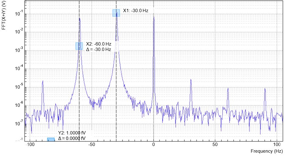
Zoom FFT
The concept of zoom FFT allows the user to analyze the spectrum of the input signal around a particular frequency by zooming in on a narrow frequency portion of the spectrum. This is done by performing a Fourier transform of the demodulated in-phase and quadrature (X and Y) components or more precisely, on the complex quantity X+iY, where i is the imaginary unit. In the LabOne user interface, this functionality is available in the Spectrum tab.
In normal FFT, the sampling rate determines the frequency span and the total acquisition time determines the frequency resolution. Having a large span and a fine resolution at the same time then requires long acquisition times at high sample rates. This means that a lot of data needs to be acquired, stored, and processed, only to retain a small portion of the spectrum and discard most of it in the end. In zoom FFT, the lock-in demodulation is used to down-shift the signal frequency, thereby allowing one to use both a much lower sampling rate and sample number to achieve the same frequency resolution. Typically, to achieve a 1 Hz frequency resolution at 1 MHz, FFT would require to collect and process approximately 106 points, while zoom FFT only processes 103 points. (Of course the high rate sampling is done by the lock-in during the demodulation stage, so the zoom FFT still needs to implicitly rely on a fast ADC.)
In order to illustrate why this is so and what benefits this measurement tool brings to the user, it is useful to remind that at the end of the demodulation of the input signal \(V_s(t)=A_s cos(\omega_s t+\tau)\), the output signal is \(X+iY=F(\omega_s-\omega_r)(A_s/\sqrt{2})e^{i\lbrack (\omega_s-\omega_r)t + \tau\rbrack}\) where F(ω) is the frequency response of the filters.
Since the demodulated signal has only one component at frequency ωs–ωr, its power spectrum (Fourier transform modulus squared) has a peak of height \((|A_s|^2/2)\cdot|F(\omega_s-\omega_r)|^2\) at ωs–ωr: this tells us the spectral power distribution of the input signal at frequencies close to ωr within the demodulation bandwidth set by the filters F(ω).
Note that:
- the ability of distinguish between positive and negative frequencies works only if the Fourier transform is done on X+iY. Had we taken X for instance, the positive and negative frequencies of its power spectrum would be equal. The symmetry relation G(–ω)=G*(ω) holds for the Fourier transform G(ω) of a real function g(t) and two identical peaks would appear at ±|ωs–ωr|.
- one can extract the amplitude of the input signal by diving the power spectrum by |F(ω)|2, the operation being limited by the numerical precision. This is implemented in LabOne and is activated by the Filter Compensation button: with the Filter Compensation enabled, the background noise appears white; without it, the effect of the filter roll-off becomes apparent.
The case of an input signal containing a single frequency component can be generalized to the case of multiple frequencies. In that case the power spectrum would display all the frequency components weighted by the filter transfer function, or normalized if the Filter Compensation is enabled.
When dealing with discrete-time signal processing, one has to be careful about aliasing which occurs when the signal frequencies higher than the sampling rate ω are not sufficiently suppressed. Remember that ω is the user settable readout rate, not the 2 GSa/s sampling rate of the GHFLI input. Since the discrete-time Fourier transform extends between –ω/2 and +ω/2, the user has to make sure that at ±ω/2 the filters provide the desired attenuation: this can be done either by increasing the sampling rate or resolving to measure a smaller frequency spectrum (i.e. with a smaller filter bandwidth).
Similarly to the continuous case, in which the acquisition time determines the maximum frequency resolution (\(2 \pi/T\) if T is the acquisition time), the resolution of the zoom FFT can be increased by increasing the number of recorded data points. If N data points are collected at a sampling rate ω, the discrete Fourier transform has a frequency resolution of ω/N.