DIO Tab
The DIO tab provides access to the settings and controls of the digital inputs and outputs. It is available on all SHFQA+ Instruments.
Features
- Monitor and control of 32-bit DIO port
- Communicate qubit states via 32-bit DIO port
- Configure Trigger Inputs and Marker Outputs
Description
The DIO tab is the main panel to control the digital inputs and outputs as well as the trigger levels. Whenever the tab is closed or an additional one of the same type is needed, clicking the following icon will open a new instance of the tab.
| Control/Tool | Option/Range | Description |
|---|---|---|
| DIO | Gives access to all controls relevant for the digital inputs and outputs including DIO, Trigger Inputs, Trigger Outputs, and Marker Outputs. |
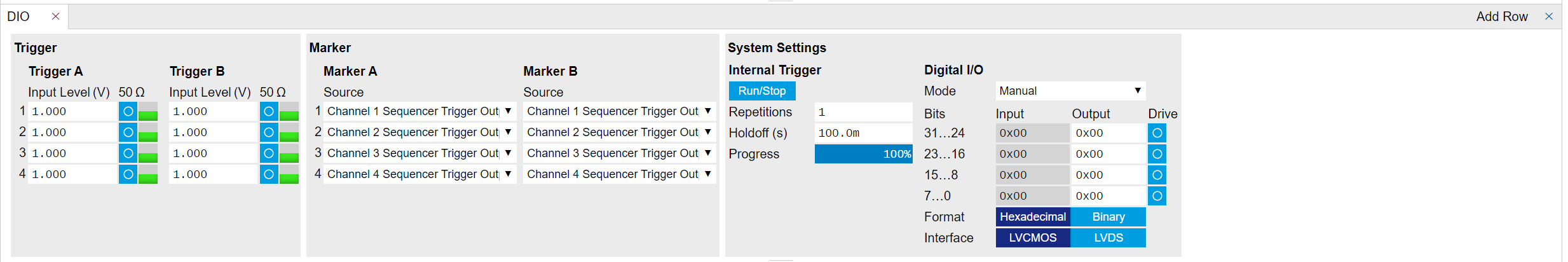
The DIO tab includes 3 sub-tabs: Trigger for configuration of trigger input level and impedance, and monitor of trigger input status on the front panel; Marker for configuration of marker source sending out from the front panel; System Settings for configuration of the internal trigger, and the 32-bit Digital I/O ports on the back panel detailed in the next section.
Digital I/O
Figure 2 shows the architecture of the DIO port. It features 32 bits that can be configured byte-wise as inputs or outputs. Even when a byte is configured as output, it works as input as well and can be read. The digital output data is synchronous to an internal clock, which is running at 50 MHz.

The DIO interface specification is detailed in the Specifications.
The Digital I/O has 3 operation modes:
-
In Manual mode, each DIO pin can be controlled manually from the UI or the API
-
In QA Sequencer N mode, each DIO pin output can be controlled by the Readout Pulse Generator Sequencer N (N indicates which Channel) with a SeqC instruction
setDIO -
In QA Results QCCS mode, DIO pins are configured to send Readout Result after Thresholding. Table 2 shows the mapping between DIO pins and input/output signals available when using the DIO connector to output qubit state measurement results. The direction is as seen from the SHFQA+ Instrument. In order to use these signals, the Digital I/O Mode and Drive setting have to be chosen accordingly.
| DIOLink signal | DIO pin | Direction | Description |
|---|---|---|---|
| VALID | DIO[0] | OUT | valid bit |
| CW | DIO[4:1] | OUT | one-hot encoding of Readout Channel |
| CW | DIO[8:23] | OUT | quantized results for a maximum of 16 State Discriminations |
| reserved | DIO[24:31] | IN | incoming communication |
Figure 3 below shows an example of multiple channel readout transmissions through DIO. Every readout is sent in a single message. A one-hot encoding of the readout channel is sent along with the readout on dedicated bits. The valid bit is set for every valid DIO transaction.

The QA Results QCCS mode of the DIO interface provides one way of communicating discriminated qubit states between 2 Instruments. For more than 2 Instruments, both qubit states and synchronization becomes essential. The following section explains how the ZSync interface works for both Instrument synchronization and feedback. Please note that ZSync settings are under the Device Tab.
ZSync Interface
The ZSync link of the Zurich Instruments' Quantum Computing Control System (QCCS) enables Instrument synchronization and communication on the system level through the Zurich Instruments' PQSC Programmable Quantum System Controller. This architecture is able to support quantum algorithms run in scalable quantum processors.
In particular, the ZSync links distribute the system clock to all Instruments and synchronize all Instruments to sub-nanosecond levels. Besides status monitoring to ensure quality and reliability of qubit tune-up routines, it provides a bidirectional data interface to send readout results to, or obtain sequence instructions from the PQSC.
The ZSync links adhere to strict real-time behavior: all data transfers are predictable to single clock cycle precision. In the SHFQA+, the link is optimized for maximum data transfer bandwidth to the central controller. For example, twice the bandwidth is reserved for results being transferred to the PQSC with respect to the allocated bandwidth for instructions that are received from the PQSC. This enables global feedback and error correction through centralized syndrome decoding and synchronized actions on the global QCCS system level.
Feedback through the PQSC
Note
More information on the ZSync, and how to properly link the SHFQA+ with the QCCS can be found in the user manual of the PQSC Programmable Quantum System Controller.
When using the startQA command, the SHFQA+ generates a readout result and forwards it to the PQSC over
the ZSync interface. The PQSC stores it in the
register bank, which handles and distributes feedback information in the QCCS system. Depending on the PQSC configuration, the results are forwarded to other devices in the
QCCS, such as the SHFSG+.
To tell the PQSC how it should forward or process the readout results, the SHFQA+ sends some additional information before the readout results:
- An Address that tells the PQSC which register of the Readout Register Bank the readout results should be directed to. This is the parameter
addressof thestartQAcommand. - An Integrators mask that indicates which integration units were activated in this readout. This is the
weighted_integrator_maskof thestartQAcommand. When Multi State Discrimination is active, the integration mask reflects the multi-state assignment.
Each component is sent in a separate ZSync message. The address is sent first, followed by the Integrators mask, and then the readout results, see Figure 4. To reduce latency, the address and the mask are sent while the readout measurement is being performed, and the readout results are then sent as soon as the discriminated qubit readout results are ready.
The readout results are sent before any averaging, so the PQSC will receive the single readout shots and not the averaged values.

Because the SHFQA+ has multiple channels, the forwarding of the readout results is interleaved to reduce latency. For example, if two readout channels perform a readout at the same time, the SHFQA+ first sends the addresses and integrator masks for both channels at the beginning of the integration. Then, it sends the readout results interleaved as soon as they are available. The order is given by the index of the QA Channel, so channel 1 goes first and so on.

If the QA Channels are not started at the same exact time, the data from the channels that start later are sent only once the data being processed are fully sent:

Functional Elements
| Control/Tool | Option/Range | Description |
|---|---|---|
| DIO mode | Select DIO mode | |
| Manual | Enables manual control of the DIO output bits. | |
| Sequencer | Enables control of DIO values by the Sequencer. | |
| Result | Sends discriminated Readout Results to the DIO. | |
| QA Results QCCS | Enables setting of DIO output values by QA results compatible with the QCCS | |
| QA Sequencer 1 | Enables setting of DIO output values by QA Sequencer 1 commands. | |
| QA Sequencer 2 | Enables setting of DIO output values by QA Sequencer 2 commands. | |
| QA Sequencer 3 | Enables setting of DIO output values by QA Sequencer 3 commands. | |
| QA Sequencer 4 | Enables setting of DIO output values by QA Sequencer 4 commands. | |
| DIO mode | Select DIO mode | |
| Manual | Enables manual control of the DIO output bits. | |
| QA Results | Sends discriminated readout results to the DIO. | |
| QA Sequencer 1 | Enables control of DIO values by the sequencer of QA channel 1. | |
| QA Result Overflow | grey/yellow/red | Red: present overflow condition on the DIO interface during readout. Yellow: indicates an overflow occurred in the past. An overflow can happen if readouts are triggered faster than the maximum possible data-rate of the DIO interface. |
| DIO bits | label | Partitioning of the 32 bits of the DIO into 4 buses of 8 bits each. Each bus can be used as an input or output. |
| DIO input | numeric value in either Hex or Binary format | Current digital values at the DIO input port. |
| DIO output | numeric value in either hexadecimal or binary format | Digital output values. Enable drive to apply the signals to the output. |
| DIO drive | ON / OFF | When on, the corresponding 8-bit bus is in output mode. When off, it is in input mode. |
| Format | Select DIO view format. | |
| Hexadecimal | DIO view format is hexadecimal. | |
| Binary | DIO view format is binary. | |
| Clock | Select DIO internal or external clocking. | |
| Interface | Selects the interface standard to use on the 32-bit DIO interface. This setting is persistent across device reboots. | |
| LVCMOS | A single-ended, 3.3V CMOS interface is used. | |
| LVDS | A differential, LVDS compatible interface is used. | |
| Trigger level | Trigger voltage level at which the trigger input toggles between low and high. Use 50% amplitude for digital input and consider the trigger hysteresis. | |
| 50 Ω | 50 Ω/1 kΩ | Trigger input impedance: When on, the trigger input impedance is 50 Ω, when off 1 kΩ. |
| Trigger Input Low status | Indicates the current low level trigger state. | |
| Off | A low state is not being triggered. | |
| On | A low state is being triggered. | |
| Trigger Input High status | Indicates the current high level trigger state. | |
| Off | A high state is not being triggered. | |
| On | A high state is being triggered. | |
| Marker output signal | Select the signal assigned to the marker output. | |
| Delay (s) | This delay adds an offset that acts only on the trigger/marker output. The total delay to the trigger/marker output is the sum of this value and the value of the output delay node. | |
| Run/Stop |  |
Enable internal trigger generator. |
| Repetitions | Number of triggers to be generated. | |
| Holdoff | Hold-off time between generated triggers. | |
| Progress | The fraction of the triggers generated so far. | |
| Synchronization | Enable synchronization. Trigger generation will only start once all synchronization participants have reported a ready status. Synchronization checks will be repeated with the same trigger generation settings (holdoff and repetitions) until synchronization is disabled. |