Specifications
Important
Unless otherwise stated, all specifications apply after 30 minutes of instrument warm-up.
Important
Important changes in the specification parameters are explicitly mentioned in the revision history of this document.
General Specifications
Table 1: General and storage
Parameter
Min
Typ
Max
storage temperature
–25 °C
-
65 °C
storage relative humidity (non-condensing)
-
-
95%
operating temperature
5 °C
-
40 °C
operating relative humidity (non-condensing)
-
-
90%
specification temperature
18 °C
-
28 °C
power consumption
-
100 W
300 W
operating environment
IEC61010, indoor location, installation category II, pollution degree 2
operating altitude
up to 2000 meters
power inlet fuses
250 V, 2 A, fast acting, 5 x 20 mm
power supply AC line
100-240 V (±10%), 50/60 Hz
dimensions (width x depth x height)
42.0 × 45 × 10 cm (with handle), 16.5 × 17.7 × 3.9 inch, 19 inch rack compatible
weight
10 kg (22 lb)
recommended calibration interval
2 years
Table 2: Maximum ratings
Parameter
Min
Typ
Max
damage threshold Signal Out
-10 V
-
+10 V
damage threshold Signal In
-3 V
-
+3 V
damage threshold Trig Out
–0.7 V
-
+4 V
damage threshold Ref/Trig In (1 kΩ input impedance)
–11 V
-
+11 V
damage threshold Ref/Trig In (50 Ω input impedance)
–6 V
-
+6 V
damage threshold Aux In (DC)
-10 V
-
+10 V
damage threshold Aux In (AC)
-3 V
-
+3 V
damage threshold External Clk In (DC)
–3 V
-
+3 V
damage threshold External Clk In (AC, with DC offset 0 V)
-1.5 V
-
+1.5 V
damage threshold External Clk Out (DC)
–3 V
-
+3 V
MDS In / Out
–0.7 V
-
+4 V
DIO In / Out in default configuration 3.3 V CMOS/TTL
–0.7 V
-
+4 V
torque limit front panel SMA connectors
-
-
0.5 Nm
torque limit back panel SMA connectors
-
-
1.0 Nm
Table 3: Host computer requirements
Parameter
Description
supported Windows operating systems
Windows 10, 11 on x86-64
supported macOS operating systems
macOS 10.11+ on x86-64 and ARMv8
supported Linux distributions
GNU/Linux (Ubuntu 14.04+, CentOS 7+, Debian 8+) on x86-64 and ARMv8
supported processors
x86-64 (Intel, AMD), ARMv8 (e.g., Raspberry Pi 4 and newer, Apple M-series)
Analog Interface Specifications
Table 4: Signal Outputs
Parameter
Details
Min
Typ
Max
connectors
-
SMA, front panel single-ended
impedance
-
-
50 Ω
-
.
coupling
-
DC
D/A converter vertical resolution
-
14 bit
D/A converter sampling rate
-
6 GSa/s
frequency range
DC
-
1.8 GHz
power range
into 50 Ω
-30 dBm
-
+5 dBm
amplitude range
into 50 Ω
10 mVpk
-
0.5 Vpk
frequency resolution
-
48 µHz
voltage spectral noise density
100 Hz, into 50 Ω
10 mVpk range
-
≤30 nV/√Hz
-
100 mVpk range
-
≤50 nV/√Hz
-
500 mVpk range
-
≤100 nV/√Hz
-
200 kHz - 200 MHz, into 50 Ω
10 mVpk range
-
≤2 nV/√Hz
-
100 mVpk range
-
≤7 nV/√Hz
-
100 mVpk range
-
≤10 nV/√Hz
-
spurious free dynamic range
1 GHz, wide band, -1 dBFS output level per range
10 mVpk range
-
> 64 dBc
-
100 mVpk range
-
> 67 dBc
-
500 mVpk range
-
> 75 dBc
-
1.8 GHz, wide band, -1 dBFS output level per range
10 mVpk range
-
> 63 dBc
-
100 mVpk range
-
> 66 dBc
-
500 mVpk range
-
> 71 dBc
-
Table 6: Demodulators
Parameter
Details
Min
Typ
Max
number of demodulators
-
8
demodulator harmonic setting range
-
1
-
1023
demodulator filter time constant
-
14 ns
-
21 s
demodulator filter bandwidth
-
3.2 mHz
-
11 MHz (with filter bypass)
demodulator filter slope/roll-off
-
6, 12, 18, 24 dB, consisting of 4 cascaded filters
data transfer
> 1 Gbit/s undisturbed connection to the host computer
Continuous
-
-
2 MSa/s
Triggered
-
-
50 MSa/s
Table 7: Auxiliary outputs and inputs
Parameter
Details
min
typ
max
high-speed auxiliary output
connectors
BNC, 4 outputs on front panel
sampling
50 MSa/s, 14 bit
bandwidth (3 dB)
15 MHz
impedance
50 Ω
amplitude (into 50 Ω)
-4 V
-
+4 V
high-precision auxiliary output
connectors
BNC, 4 outputs on front panel
sampling
1 MSa/s, 18 bit
bandwidth (3 dB)
200 kHz
impedance
50 Ω
amplitude (into 50 Ω)
-4 V
-
+4 V
Table 8: Trigger Outputs & Inputs
Parameter
Details
Min
Typ
Max
trigger outputs
-
1 per channel, SMA output on front panel
trigger output high voltage
-
-
3.3 V
-
trigger output low voltage
-
-
0 V
-
trigger output impedance
-
-
50 Ω
-
trigger output rise time 20% to 80%
-
-
300 ps
-
trigger output period jitter
square wave, 100 MHz
-
60 ps p-p
-
trigger inputs
-
2 per channel, 2 SMA on front panel
trigger input impedance
-
50 Ω / 1 kΩ
trigger input voltage range
50 Ω impedance
–5 V
-
5 V
1 kΩ impedance
–10 V
-
10 V
trigger input threshold range
50 Ω impedance
–5 V
-
5 V
1 kΩ impedance
–10 V
-
10 V
trigger input threshold resolution
-
-
< 0.4 mV
-
trigger input threshold hysteresis
-
-
> 60 mV
-
trigger input min. pulse width
-
-
5 ns
-
trigger input max. operating frequency
-
-
300 MHz
-
Table 9: Other Inputs and Outputs
Parameter
Details
min
Typ
Max
reference clock input
-
SMA on back panel
reference clock input impedance
-
50 Ω, AC coupled
reference clock input frequency
-
10 / 100 MHz
reference clock input amplitude
10 MHz
-4 dBm
-
+13 dBm
100 MHz
–5 dBm
-
+13 dBm
reference clock output
-
SMA on back panel
reference clock output impedance
50 Ω, AC coupled
reference clock output amplitude
into 50 Ω
2 Vpp
-
5 Vpp
reference clock output frequency
10/100 MHz
reference clock output jitter
derived from integrated phase noise measurement (12 kHz to 20 MHz offset frequency)
-
280 fs RMS
-
Table 10: Oscillator and Clocks
Parameter
Details
Min
Typ
Max
internal clock type
-
OCXO
internal clock long term accuracy / aging
-
-
-
±0.3 ppm/year
internal clock short term stability (1 s)
-
-
-
±0.05 ppm
internal clock initial accuracy
-
-
-
±0.5 ppm
internal clock temperature stability
–20°C to 70°C
-
-
±0.5 ppm
internal clock phase noise
offset 100 Hz
-
–135 dBc/Hz
-
offset 1 kHz
-
–157 dBc/Hz
-
Digital Interface Specifications
Table 11: Digital Interfaces
Parameter
Description
host computer connection
USB 3.0, 1.6 Gbit/s (1 communication, 1 maintenance)
1GbE, LAN / Ethernet, 1 Gbit/s
DIO port
4 x 8 bit, general purpose digital input/output port, 3.3 V TTL specification
ZSync peripheral port
connector for ZI proprietary bus to communicate with external peripherals (2 times)
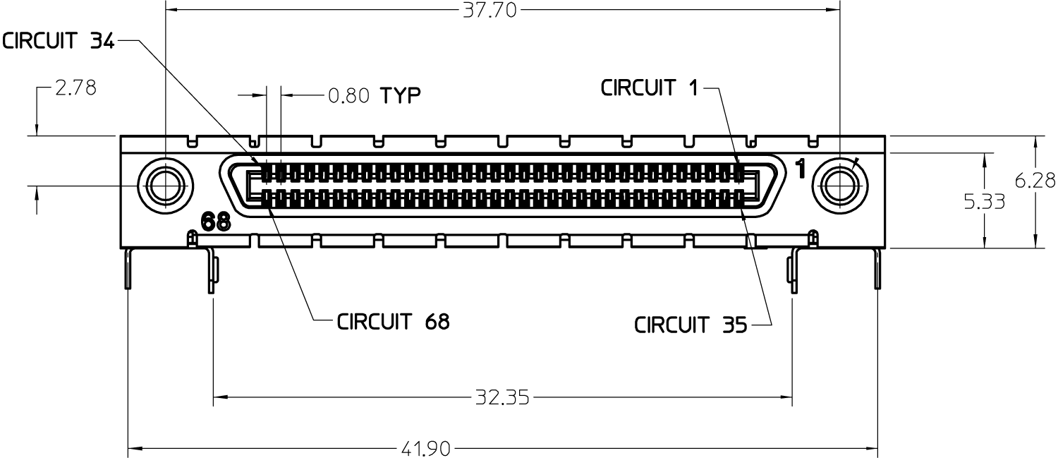
DIO Port
The DIO port is a VHDCI 68 pin connector as introduced by the SPI-3
document of the SCSI-3 specification. It is a female connector that
requires a 32 mm wide male connector. The interface standard is
switchable between LVDS (low-voltage differential signalling) and
LVCMOS/LVTTL. The DIO port features 32 user-controlled bits that can all
be configured byte-wise as inputs or outputs in LVCMOS/LVTTL mode,
whereas in LVDS mode, half of the bits are always configured as inputs.
For more specifics on how the user-definable pins can be set.
Figure 1: DIO HD 68 pin connector
Table 12: Electrical Specifications
Parameter
Details
Min
Typ
Max
supported DIO interface standards
-
LVCMOS/LVTTL (single-ended, 3.3 V); LVDS (differential)
high-level input voltage VIH
LVCMOS/LVTTL
2.0 V
-
-
low-level input voltage VIL
LVCMOS/LVTTL
-
-
0.8 V
high-level output voltage VOH
LVCMOS/LVTTL
2.6 V
-
-
low-level output voltage VOL
LVCMOS/LVTTL
-
-
0.4 V
high-level output current IOH (sourcing)
LVCMOS/LVTTL
-
-
12 mA
low-level output current IOL (sinking)
LVCMOS/LVTTL
-
-
12 mA
input differential voltage VID
LVDS
100 mV
-
600 mV
input common-mode voltage VICM
LVDS
0.3 V
-
2.35 V
output differential voltage VOD
LVDS
247 mV
-
454 mV
output common-mode voltage VOCM
LVDS
1.125 V
-
1.375 V
Table 13: DIO Pin Assignment in LVCMOS/LVTTL Mode
Pin
Name
Description
68
CLKI
digital input
67
unused
leave unconnected
66 .. 59
DIO[31:24]
digital input or output byte (set by user)
58 .. 51
DIO[23:16]
digital input or output byte (set by user)
50 .. 43
DIO[15:8]
digital input or output byte (set by user)
42 .. 35
DIO[7:0]
digital input or output byte (set by user)
34
GND
digital ground
33
unused
leave unconnected
32 .. 1
GND
digital ground
Table 14: DIO Pin Assignment in LVDS Mode
Pin
Name
Description
68
CLKI+
digital input
67
unused
leave unconnected
66 .. 59
DI+[31:24]
digital input byte
58 .. 51
DI+[23:16]
digital input byte
50 .. 43
DIO+[15:8]
digital input or output byte (set by user)
42 .. 35
DIO+[7:0]
digital input or output byte (set by user)
34
CLKI–
digital input
33
unused
leave unconnected
32 .. 25
DI–[31:24]
digital input byte
24 .. 17
DI–[23:16]
digital input byte
16 .. 9
DIO–[15:8]
digital input or output byte (set by user)
8 .. 1
DIO–[7:0]
digital input or output byte (set by user)