DIO Tab
The DIO tab provides access to the settings and controls of the digital inputs and outputs. It is available on all SHFSG+ Instruments.
Features
- Monitor and control of 32-bit DIO port
- Configure Trigger Inputs and Marker Outputs
- Configure the Internal Trigger settings
Description
The DIO tab is the main panel to control the digital inputs and outputs as well as the trigger levels. Whenever the tab is closed or an additional one of the same type is needed, clicking the following icon will open a new instance of the tab.
| Control/Tool | Option/Range | Description |
|---|---|---|
| DIO | Gives access to all controls relevant for the digital inputs and outputs including DIO, Trigger Inputs, Trigger Outputs, and Marker Outputs. |
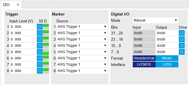
The Digital I/O section provides numerical monitors to observe the states of the digital inputs and outputs.
The Trigger section shows the settings for the 2, 4 or 8 Trig inputs on the front panel. The LED status indicator helps in monitoring the input signal state and selecting the threshold.
The Marker section allows users to assign internal trigger signal or the marker bits to the 2, 4 or 8 Mark outputs on the front panel. Alternatively, the outputs can be set to static high or low values. The marker outputs have a configurable delay, with a resolution of 1 ns.
In the Internal Trigger section, the number of repetitions and the holdoff time of the Internal Trigger can be configured. The Internal Trigger is useful for synchronizing the outputs of different channels on the same instrument. The Synchronization checkbox enable the synchronization check for the internal trigger.
Digital I/O
Figure 2 shows the architecture of the DIO port. It features 32 bits that can be configured byte-wise as inputs or outputs. Even when a byte is configured as output, it works as input as well and can be read. The digital output data is synchronous to an internal clock, which is running at 50 MHz.

The DIO interface specification is detailed in the Specifications.
The Digital I/O has 2 operation modes:
-
In Manual mode, each DIO pin can be controlled manually from the UI or the API
-
In AWG Sequencer N mode, each DIO pin output can be controlled by the AWG Sequencer N (N indicates which Channel) with a SeqC instruction
setDIO
ZSync Interface
The ZSync link of the Zurich Instruments' Quantum Computing Control System (QCCS) enables Instrument synchronization and communication on the system level through the Zurich Instruments' PQSC Programmable Quantum System Controller. This architecture is able to support quantum algorithms run in scalable quantum processors.
In particular, the ZSync links distribute the system clock to all Instruments and synchronize all Instruments to sub-nanosecond levels. Besides status monitoring to ensure quality and reliability of qubit tune-up routines, it provides a bidirectional data interface to send readout results to, or obtain sequence instructions from the PQSC or QHub.
The ZSync links adhere to strict real-time behavior: all data transfers are predictable to single clock cycle precision. This enables global feedback and error correction through centralized syndrome decoding and synchronized actions on the global QCCS system level.
Feedback through the PQSC
Note
More information on the ZSync, and how to properly link the SHFSG+ with the QCCS can be found in the user manual of the PQSC Programmable Quantum System Controller.
Using the startQA- command, the SHFQA+ or the Quantum Analyzer Channel
of the SHFQC+ generates a readout result and forwards it to the PQSC over
the ZSync. Depending on the address provided, the PQSC stores it in the
register bank - the center of the feedback in the QCCS system. After
processing, the PQSC then forwards the results to other devices in the
QCCS, such as the SHFSG+.
Functional Elements
| Control/Tool | Option/Range | Description |
|---|---|---|
| DIO mode | Select DIO mode | |
| Manual | Enables manual control of the DIO output bits. | |
| Sequencer | Enables control of DIO values by the Sequencer. | |
| Result | Sends discriminated Readout Results to the DIO. | |
| DIO mode | Select DIO mode | |
| Manual | Enables manual control of the DIO output bits. | |
| SG Sequencer 1 | Enables control of DIO values by the sequencer of SG channel 1. | |
| SG Sequencer 2 | Enables control of DIO values by the sequencer of SG channel 2. | |
| SG Sequencer 3 | Enables control of DIO values by the sequencer of SG channel 3. | |
| SG Sequencer 4 | Enables control of DIO values by the sequencer of SG channel 4. | |
| SG Sequencer 5 | Enables control of DIO values by the sequencer of SG channel 5. | |
| SG Sequencer 6 | Enables control of DIO values by the sequencer of SG channel 6. | |
| QA Result Overflow | grey/yellow/red | Red: present overflow condition on the DIO interface during readout. Yellow: indicates an overflow occurred in the past. An overflow can happen if readouts are triggered faster than the maximum possible data-rate of the DIO interface. |
| DIO bits | label | Partitioning of the 32 bits of the DIO into 4 buses of 8 bits each. Each bus can be used as an input or output. |
| DIO input | numeric value in either Hex or Binary format | Current digital values at the DIO input port. |
| DIO output | numeric value in either hexadecimal or binary format | Digital output values. Enable drive to apply the signals to the output. |
| DIO drive | ON / OFF | When on, the corresponding 8-bit bus is in output mode. When off, it is in input mode. |
| Format | Select DIO view format. | |
| Hexadecimal | DIO view format is hexadecimal. | |
| Binary | DIO view format is binary. | |
| Clock | Select DIO internal or external clocking. | |
| Interface | Selects the interface standard to use on the 32-bit DIO interface. This setting is persistent across device reboots. | |
| LVCMOS | A single-ended, 3.3V CMOS interface is used. | |
| LVDS | A differential, LVDS compatible interface is used. | |
| Trigger level | Trigger voltage level at which the trigger input toggles between low and high. Use 50% amplitude for digital input and consider the trigger hysteresis. | |
| 50 Ω | 50 Ω/1 kΩ | Trigger input impedance: When on, the trigger input impedance is 50 Ω, when off 1 kΩ. |
| Trigger Input Low status | Indicates the current low level trigger state. | |
| Off | A low state is not being triggered. | |
| On | A low state is being triggered. | |
| Trigger Input High status | Indicates the current high level trigger state. | |
| Off | A high state is not being triggered. | |
| On | A high state is being triggered. | |
| Marker output signal | Select the signal assigned to the marker output. | |
| Delay (s) | This delay adds an offset that acts only on the trigger/marker output. The total delay to the trigger/marker output is the sum of this value and the value of the output delay node. | |
| Run/Stop |  |
Enable internal trigger generator. |
| Repetitions | Number of triggers to be generated. | |
| Holdoff | Hold-off time between generated triggers. | |
| Progress | The fraction of the triggers generated so far. | |
| Synchronization | Enable synchronization. Trigger generation will only start once all synchronization participants have reported a ready status. Synchronization checks will be repeated with the same trigger generation settings (holdoff and repetitions) until synchronization is disabled. |